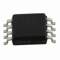
W25Q16BVSSIG Winbond Electronics, W25Q16BVSSIG Datasheet - Page 30

W25Q16BVSSIG
Manufacturer Part Number
W25Q16BVSSIG
Description
IC SPI FLASH 16MBIT 8SOIC
Manufacturer
Winbond Electronics
Datasheet
1.W25Q16BVSFIG.pdf
(68 pages)
Specifications of W25Q16BVSSIG
Format - Memory
FLASH
Memory Type
FLASH
Memory Size
16M (2M x 8)
Speed
104MHz
Interface
SPI Serial
Voltage - Supply
2.7 V ~ 3.6 V
Operating Temperature
-40°C ~ 85°C
Package / Case
8-SOIC (5.3mm Width), 8-SOP, 8-SOEIAJ
Lead Free Status / RoHS Status
Lead free / RoHS Compliant
Available stocks
Company
Part Number
Manufacturer
Quantity
Price
Company:
Part Number:
W25Q16BVSSIG
Manufacturer:
WINBOND
Quantity:
9 270
Company:
Part Number:
W25Q16BVSSIG
Manufacturer:
WINBOND
Quantity:
20 655
Part Number:
W25Q16BVSSIG
Manufacturer:
WINBOND/华邦
Quantity:
20 000
11.2.14 Fast Read Quad I/O (EBh)
The Fast Read Quad I/O (EBh) instruction is similar to the Fast Read Dual I/O (BBh) instruction except
that address and data bits are input and output through four pins IO
clocks are required prior to the data output
allowing faster random access for code execution (XIP) directly from the Quad SPI. The Quad Enable bit
(QE) of Status Register-2 must be set to enable the Fast read Quad I/O Instruction.
Fast Read Quad I/O with “Continuous Read Mode”
The Fast Read Quad I/O instruction can further reduce instruction overhead through setting the
“Continuous Read Mode” bits (M7-0) after the input Address bits (A23-0), as shown in figure 13a. The
upper nibble of the (M7-4) controls the length of the next Fast Read Quad I/O instruction through the
inclusion or exclusion of the first byte instruction code. The lower nibble bits of the (M3-0) are don’t care
(“x”). However, the IO pins should be high-impedance prior to the falling edge of the first data out clock.
If the “Continuous Read Mode” bits (M7-0) equals “Ax” hex, then the next Fast Read Quad I/O instruction
(after /CS is raised and then lowered) does not require the EBh instruction code, as shown in figure 13b.
This reduces the instruction sequence by eight clocks and allows the Read address to be immediately
entered after /CS is asserted low. If the “Continuous Read Mode” bits (M7-0) are any value other than
“Ax” hex, the next instruction (after /CS is raised and then lowered) requires the first byte instruction code,
thus returning to normal operation. A “Continuous Read Mode” Reset instruction can be used to reset
(M7-0) before issuing normal instructions (See 11.2.32 for detailed descriptions).
Figure 13a. Fast Read Quad I/O Instruction Sequence Diagram (M7-0 = 0xh or NOT Axh)
.
The Quad I/O dramatically reduces instruction overhead
- 30 -
0
, IO
1
, IO
2
Byte 1
Byte 1
and IO
W25Q16BV
Byte 2
Byte 2
3
and four Dummy


