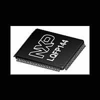
LPC2212_2214 NXP Semiconductors, LPC2212_2214 Datasheet - Page 8

LPC2212_2214
Manufacturer Part Number
LPC2212_2214
Description
The LPC2212/2214 are based on a 16/32-bit ARM7TDMI-S CPU with real-time emulationand embedded trace support, together with 128/256 kB of embedded high-speed flashmemory
Manufacturer
NXP Semiconductors
Datasheet
1.LPC2212_2214.pdf
(47 pages)
NXP Semiconductors
Table 3.
LPC2212_2214
Product data sheet
Symbol
P0[30]/AIN3/EINT3/
CAP0[0]
P1[0] to P1[31]
P1[0]/CS0
P1[1]/OE
P1[16]/TRACEPKT0
P1[17]/TRACEPKT1
P1[18]/TRACEPKT2
P1[19]/TRACEPKT3
P1[20]/TRACESYNC
P1[21]/PIPESTAT0
P1[22]/PIPESTAT1
P1[23]/PIPESTAT2
P1[24]/TRACECLK
P1[25]/EXTIN0
P1[26]/RTCK
P1[27]/TDO
P1[28]/TDI
P1[29]/TCK
P1[30]/TMS
P1[31]/TRST
P2[0] to P2[31]
P2[0]/D0
P2[1]/D1
P2[2]/D2
P2[3]/D3
P2[4]/D4
P2[5]/D5
P2[6]/D6
Pin description
Pin
33
91
90
34
24
15
7
102
95
86
82
70
60
52
144
140
126
113
43
98
105
106
108
109
114
115
…continued
Type Description
I
I
I
I/O
O
O
O
O
O
O
O
O
O
O
O
I
I/O
O
I
I
I
I
I/O
I/O
I/O
I/O
I/O
I/O
I/O
I/O
All information provided in this document is subject to legal disclaimers.
AIN3 — ADC, input 3. This analog input is always connected to its pin.
EINT3 — External interrupt 3 input.
CAP0[0] — Capture input for Timer 0, channel 0.
Port 1 is a 32-bit bidirectional I/O port with individual direction controls for
each bit. The operation of port 1 pins depends upon the pin function selected
via the Pin Connect Block.
Pins 2 through 15 of port 1 are not available.
LOW-active Chip Select 0 signal.
(Bank 0 addresses range 0x8000 0000 to 0x80FF FFFF)
LOW-active Output Enable signal.
Trace Packet, bit 0. Standard I/O port with internal pull-up.
Trace Packet, bit 1. Standard I/O port with internal pull-up.
Trace Packet, bit 2. Standard I/O port with internal pull-up.
Trace Packet, bit 3. Standard I/O port with internal pull-up.
Trace Synchronization; standard I/O port with internal pull-up.
Note: LOW on this pin while RESET is LOW, enables pins P1[25:16] to
operate as Trace port after reset.
Pipeline Status, bit 0. Standard I/O port with internal pull-up.
Pipeline Status, bit 1. Standard I/O port with internal pull-up.
Pipeline Status, bit 2. Standard I/O port with internal pull-up.
Trace Clock. Standard I/O port with internal pull-up.
External Trigger Input. Standard I/O with internal pull-up.
Returned Test Clock output. Extra signal added to the JTAG port. Assists
debugger synchronization when processor frequency varies. Bidirectional pin
with internal pull-up.
Note: LOW on this pin while RESET is LOW, enables pins P1[31:26] to
operate as Debug port after reset.
Test Data out for JTAG interface.
Test Data in for JTAG interface.
Test Clock for JTAG interface. This clock must be slower than
clock (CCLK) for the JTAG interface to operate.
Test Mode Select for JTAG interface.
Test Reset for JTAG interface.
Port 2 is a 32-bit bidirectional I/O port with individual direction controls for
each bit. The operation of port 2 pins depends upon the pin function selected
via the Pin Connect Block.
External memory data line 0.
External memory data line 1.
External memory data line 2.
External memory data line 3.
External memory data line 4.
External memory data line 5.
External memory data line 6.
Rev. 5 — 14 June 2011
Single-chip 16/32-bit ARM microcontrollers
LPC2212/2214
© NXP B.V. 2011. All rights reserved.
1
⁄
6
of the CPU
8 of 47


