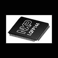
LPC2212_2214 NXP Semiconductors, LPC2212_2214 Datasheet - Page 23

LPC2212_2214
Manufacturer Part Number
LPC2212_2214
Description
The LPC2212/2214 are based on a 16/32-bit ARM7TDMI-S CPU with real-time emulationand embedded trace support, together with 128/256 kB of embedded high-speed flashmemory
Manufacturer
NXP Semiconductors
Datasheet
1.LPC2212_2214.pdf
(47 pages)
NXP Semiconductors
LPC2212_2214
Product data sheet
CAUTION
6.18.4 Code security (Code Read Protection - CRP)
6.18.5 External interrupt inputs
functions are turned off for any reason. Since the oscillator and other functions are turned
off during Power-down mode, any wake-up of the processor from Power-down mode
makes use of the Wake-up Timer.
The Wake-up Timer monitors the crystal oscillator as the means of checking whether it is
safe to begin code execution. When power is applied to the chip, or some event caused
the chip to exit Power-down mode, some time is required for the oscillator to produce a
signal of sufficient amplitude to drive the clock logic. The amount of time depends on
many factors, including the rate of V
and its electrical characteristics (if a quartz crystal is used), as well as any other external
circuitry (e.g., capacitors), and the characteristics of the oscillator itself under the existing
ambient conditions.
This feature of the LPC2212/2214 allows the user to enable different levels of security in
the system so that access to the on-chip flash and use of the JTAG and ISP can be
restricted. When needed, CRP is invoked by programming a specific pattern into a
dedicated flash location. IAP commands are not affected by the CRP.
There are three levels of the Code Read Protection.
CRP1 disables access to chip via the JTAG and allows partial flash update (excluding
flash sector 0) using a limited set of the ISP commands. This mode is useful when CRP is
required and flash field updates are needed but all sectors can not be erased.
CRP2 disables access to chip via the JTAG and only allows full flash erase and update
using a reduced set of the ISP commands.
Running an application with level CRP3 selected fully disables any access to chip via the
JTAG pins and the ISP. This mode effectively disables ISP override using P0[14] pin, too.
It is up to the user’s application to provide (if needed) flash update mechanism using IAP
calls or call reinvoke ISP command to enable flash update via UART0.
Remark: Devices without the suffix /00 or /01 have only a security level equivalent to
CRP2 available.
The LPC2212/2214 include up to nine edge or level sensitive External Interrupt Inputs as
selectable pin functions. When the pins are combined, external events can be processed
as four independent interrupt signals. The External Interrupt Inputs can optionally be used
to wake up the processor from Power-down mode.
If level three Code Read Protection (CRP3) is selected, no future factory testing can be
performed on the device.
All information provided in this document is subject to legal disclaimers.
Rev. 5 — 14 June 2011
DD
ramp (in the case of power on), the type of crystal
Single-chip 16/32-bit ARM microcontrollers
LPC2212/2214
© NXP B.V. 2011. All rights reserved.
23 of 47


