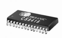
CS8416-CNZ Cirrus Logic Inc, CS8416-CNZ Datasheet - Page 13

CS8416-CNZ
Manufacturer Part Number
CS8416-CNZ
Description
IC RCVR DGTL 192KHZ 28QFN COMM
Manufacturer
Cirrus Logic Inc
Type
Digital Audio Interface Receiverr
Datasheet
1.CS8416-CZZ.pdf
(60 pages)
Specifications of CS8416-CNZ
Applications
Digital Audio
Mounting Type
Surface Mount
Package / Case
28-QFN
Audio Control Type
Digital
Control Interface
I2C, SPI
Control / Process Application
AV & DVD Receivers, CD-R, Digital Mixing Consoles
Supply Voltage Range
3.13V To 5.25V, 3.13V To 3.46V
Lead Free Status / RoHS Status
Lead free / RoHS Compliant
For Use With
598-1017 - BOARD EVAL FOR CS8416 RCVR
Lead Free Status / RoHS Status
Lead free / RoHS Compliant, Lead free / RoHS Compliant
Other names
598-1723
DS578F3
AD0 / CS
SDOUT
CDOUT
OSCLK
OLRCK
Name
OMCK
RMCK
CCLK
GPO2
GPO1
GPO0
SDA /
SCL /
AD1 /
CDIN
AD2 /
RXN
Pin
Pin #
25
24
27
28
26
17
16
14
15
18
19
20
5
Negative AES3/SPDIF Input (Input) - Single-ended or differential receiver input carrying AES3 or
S/PDIF encoded digital data. Used along with RXP[7:0] to form an AES3 differential input. In single-
ended operation this should be AC coupled to ground through a capacitor. See
AES3/SPDIF/IEC60958 Receiver Components” on page 49
System Clock (Input) - When the OMCK System Clock Mode is enabled using the SWCLK bit in the
Control 1 register, the clock signal input on this pin is automatically output through RMCK on PLL unlock.
OMCK serves as the reference signal for OMCK/RMCK ratio expressed in register 18h.
Clock Mode” section on page 28
Input Section Recovered Master Clock (Output) - Input section recovered master clock output from
the PLL. Frequency defaults to 256x the sample rate (F
in the Control 1 register (01h). RMCK may also be set to high impedance by the RXD bit in the Control 4
register (04h).
Serial Audio Output Bit Clock (Input/Output) - Serial bit clock for audio data on the SDOUT pin
Serial Audio Output Left/Right Clock (Input/Output) - Word rate clock for the audio data on the
SDOUT pin. Frequency will be the output sample rate (Fs)
Serial Audio Output Data (Output) - Audio data serial output pin. This pin must be pulled high to VL
through a 47 kΩ resistor to place the part in Software Mode.
Serial Control Data I/O (I²C) / Data Out (SPI) (Input/Output) - In I²C Mode, SDA is the control I/O data
line. SDA is open drain and requires an external pull-up resistor to VL. In SPI Mode, CDOUT is the out-
put data from the control port interface on the CS8416. See the
page
Control Port Clock (Input) - Serial control interface clock and is used to clock control data bits into and
out of the CS8416. CCLK is an open drain output and requires an external pull-up resistor to VL. See the
“Control Port Description” section on page
Address Bit 0 (I²C) / Control Port Chip Select (SPI) (Input) - A falling edge on this pin puts the CS8416
into SPI Control Port Mode. With no falling edge, the CS8416 defaults to I²C Mode. In I²C Mode, AD0 is
a chip address pin. In SPI Mode, CS is used to enable the control port interface on the CS8416. See the
“Control Port Description” section on page
Address Bit 1 (I²C) / Serial Control Data in (SPI) (Input) - In I²C Mode, AD1 is a chip address pin. In
SPI Mode, CDIN is the input data line for the control port interface. See the
section on page
General Purpose Output 2 (Output) - If using the I²C control port, this pin must be pulled high or low
through a 47 kΩ resistor. See the
Outputs” on page 29
General Purpose Output 1 (Output) - See
General Purpose Output 0 (Output) - See
33.
33.
for GPO functions.
“Control Port Description” section on page 33
Pin Description
33.
33.
“General Purpose Outputs” on page 29
“General Purpose Outputs” on page 29
s
) and may be set to 128x through the RMCKF bit
for recommended input circuits.
“Control Port Description” section on
“Control Port Description”
“External
and
for GPO functions.
for GPO functions.
“General Purpose
“OMCK System
CS8416
13


