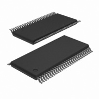
SC28L202A1DGG,118 NXP Semiconductors, SC28L202A1DGG,118 Datasheet - Page 65

SC28L202A1DGG,118
Manufacturer Part Number
SC28L202A1DGG,118
Description
IC UART DUAL W/FIFO 56-TSSOP
Manufacturer
NXP Semiconductors
Series
IMPACTr
Datasheet
1.SC28L202A1DGG118.pdf
(77 pages)
Specifications of SC28L202A1DGG,118
Features
False-start Bit Detection
Number Of Channels
2, DUART
Fifo's
256 Byte
Voltage - Supply
3.3V, 5V
With Parallel Port
Yes
With Auto Flow Control
Yes
With False Start Bit Detection
Yes
With Modem Control
Yes
With Cmos
Yes
Mounting Type
Surface Mount
Package / Case
56-TFSOP (0.240", 6.10mm Width)
Lead Free Status / RoHS Status
Lead free / RoHS Compliant
Other names
935276109118
SC28L202A1DGG-T
SC28L202A1DGG-T
SC28L202A1DGG-T
SC28L202A1DGG-T
Available stocks
Company
Part Number
Manufacturer
Quantity
Price
Company:
Part Number:
SC28L202A1DGG,118
Manufacturer:
EPCOS
Quantity:
12 000
Philips Semiconductors
AC CHARACTERISTICS
V
2005 Nov 01
Symbol
Reset timing (See Figures 4, 5)
t
Bus Timing (See Figure 6)
t
t
t
t
t
t
t
t
t
t
t
Port Timing (See Figure 10)
t
t
t
Interrupt Timing (See Figure 11)
t
Clock Timing (See Figures 12, 13, 14)
t
f
t
f
t
f
t
f
Transmitter Timing (See Figures 13, 15)
t
t
Receiver Timing (See Figures 14, 16)
t
t
CC
RES
AS
AH
CS
CH
RW
DD
DA
DF
DS
DH
RWD
PS
PH
PD
IR
CLK
CLK
CTC
CTC
RX
RX
TX
TX
TXD
TCS
RXS
RXH
Dual UART
= 3.3 V
10%; T
Parameter
Reset Pulse Width
A6–A0 set-up time to RDN, WRN Low
A6–A0 hold time from RDN, WRN low
CEN set-up time to RDN, WRN LOW
CEN Hold time from RDN, WRN HIGH
WRN, RDN pulse width (Low time)
Data valid after RDN low (125 pF load) See load table for smaller loads
RDN low to data bus active
Data bus floating after RDN or CEN high
Data bus set-up time before WRN or CEN high (write cycle)
Data hold time after WRN high
High time between read and/or write cycles
Port in set-up time before RDN low (Read IP ports cycle)
Port in hold time after RDN high
OP port valid after WRN or CEN high (OPR write cycle)
INTRN (or I/O(7:3)B when used as interrupts) negated from:
X1/SCLK high or low time
X1/SCLK frequency (7.0 to 16.2 MHz with crystal)
C/T Clk (IP2) high or low time (C/T external clock input)
C/T Clk (IP2) frequency
RxC high or low time (16X)
RxC Frequency (16X)
RxC Frequency (1x)
TxC High or low time (16X)
TxC frequency (16X)
TxC frequency (1X)
TxD output delay from TxC low (TxC input pin)
Output delay from TxC output pin low to TxD data output
RxD data set-up time to RxC high
RxD data hold time from RxC high
Read RxFIFO (RxRDY/FFULL interrupt)
Write TxFIFO (TxRDY interrupt)
Reset Command (delta break change interrupt)
Stop C/T command (Counter/timer interrupt
Read IPCR (delta input port change interrupt)
Write IMR (Clear of change interrupt mask bit(s))
amb
= – 40 C to +85 C unless otherwise specified
1, 2, 3
(NOMINAL 3.3 V)
59
LIMITS
Min
100
10
10
0
0
40
–
0
–
15
0
10
0
0
–
–
–
–
–
–
–
10
1
10
0
10
0
0
10
0
0
–
–
20
20
4
Typ
–
–
–
–
–
–
–
–
–
–
–
–
–
–
–
–
–
–
–
–
–
–
–
–
–
–
–
–
–
–
–
–
–
–
–
SC28L202
Max
–
–
–
–
–
–
40
–
15
–
–
–
–
–
40
40
40
40
40
40
40
–
34
–
8
–
24
1.5
–
24
1.5
40
40
–
–
Product data sheet
UNIT
ns
ns
ns
ns
ns
ns
ns
ns
ns
ns
ns
ns
ns
ns
ns
ns
ns
ns
ns
ns
ns
ns
MHz
ns
MHz
ns
MHz
MHz
ns
MHz
MHz
ns
ns
ns
ns


