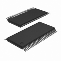
SC28L202A1DGG,118 NXP Semiconductors, SC28L202A1DGG,118 Datasheet - Page 64

SC28L202A1DGG,118
Manufacturer Part Number
SC28L202A1DGG,118
Description
IC UART DUAL W/FIFO 56-TSSOP
Manufacturer
NXP Semiconductors
Series
IMPACTr
Datasheet
1.SC28L202A1DGG118.pdf
(77 pages)
Specifications of SC28L202A1DGG,118
Features
False-start Bit Detection
Number Of Channels
2, DUART
Fifo's
256 Byte
Voltage - Supply
3.3V, 5V
With Parallel Port
Yes
With Auto Flow Control
Yes
With False Start Bit Detection
Yes
With Modem Control
Yes
With Cmos
Yes
Mounting Type
Surface Mount
Package / Case
56-TFSOP (0.240", 6.10mm Width)
Lead Free Status / RoHS Status
Lead free / RoHS Compliant
Other names
935276109118
SC28L202A1DGG-T
SC28L202A1DGG-T
SC28L202A1DGG-T
SC28L202A1DGG-T
Available stocks
Company
Part Number
Manufacturer
Quantity
Price
Company:
Part Number:
SC28L202A1DGG,118
Manufacturer:
EPCOS
Quantity:
12 000
1. Parameters are valid over specified temperature range.
2. All voltage measurements are referenced to ground (GND). For testing, all inputs swing between 0.4 V and 3.0 V with a transition time of
3. Typical values are at +25 C, typical supply voltages, and typical processing parameters.
4. Test conditions for outputs: C
5. I/O port pins have active pull-up transistors that will source a typical 2 A from V
6. All outputs are disconnected. Inputs are switching between CMOS levels of V
Philips Semiconductors
DC ELECTRICAL CHARACTERISTICS
V
NOTES:
2005 Nov 01
SYMBOL
V
V
V
V
V
I
I
I
I
I
I
I
I
I
CC
IX1PD
ILX1
IHX1
i
OZH
OZL
ODL
ODH
CC
IL
IH
IH
OL
OH
Dual UART
5 ns maximum. For X1/SCLK this swing is between 0.4 V and 4.4 V. All time measurements are referenced at input voltages of 0.8 V and
2.0 V and output voltages of 0.8 V and 2.0 V, as appropriate.
= 3.3 V
PARAMETER
Input low voltage
Input high voltage (X1/SCLK)
Input high voltage (X1/SCLK)
Output low voltage
Output high voltage (except OD outputs)
X1/SCLK input current – power down
X1/SCLK input low current – operating
X1/SCLK input high current – operating
Input leakage current
Output off current high, 3–State data bus
Output off current low, 3–State data bus
Open–drain output low current in off–state
Open–drain output high current in off–state
Power supply current
10%; T
I/O port pins and IACKN
All other pins
Operating mode
Power down mode
amb
= – 40 C to +85 C unless otherwise specified
5
L
= 85 pF, except interrupt outputs. Test conditions for interrupt outputs: C
6
1, 2, 3
4
(NOMINAL 3.3 V)
TEST CONDITIONS
I
I
V
V
V
V
V
V
V
V
V
CMOS input levels; freq. = 10 MHz
CMOS input levels; freq. = 0 MHz
OL
OH
IN
IN
IN
IN
IN
IN
IN
IN
IN
= 4 mA
= –400 A
= 0 V to V
= 0 V
= V
= 0 V to V
= 0 V to V
= V
= 0 V
= 0 V
= V
CC
CC
CC
58
CC
CC
CC
CC
CC
– 0.2 V and V
when they are at V
SS
+ 0.2 V.
LIMITS
Min
–
0.8*V
2.4
–
V
–1
–30
0
–10
–1
0
–5
–10
–
–
–
CC
SS
L
= 85 pF, R
–0.5
. These pins at V
CC
Typ
–
–
–
–
–
–
–
–
–
–
–
–
–
–
9
200
L
= 2.7 k to V
SC28L202
CC
Product data sheet
Max
0.2*V
–
–
0.4
–
1
0
30
1
1
5
–
–
1
20
500
source 0.0 A.
CC
CC
.
UNIT
V
V
V
V
V
mA
A
A
A
A
A
A
A
A
A
A


