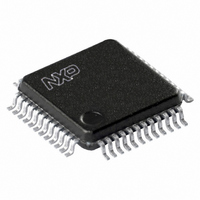
SC68C2550BIB48,151 NXP Semiconductors, SC68C2550BIB48,151 Datasheet - Page 9

SC68C2550BIB48,151
Manufacturer Part Number
SC68C2550BIB48,151
Description
IC UART DUAL W/FIFO 48-LQFP
Manufacturer
NXP Semiconductors
Type
5 V, 3.3 V and 2.5 V dual UART, 5 Mbit/s with 16-byte FIFOsr
Datasheet
1.SC68C2550BIB48151.pdf
(36 pages)
Specifications of SC68C2550BIB48,151
Number Of Channels
2, DUART
Package / Case
48-LQFP
Features
False-start Bit Detection
Fifo's
16 Byte
Voltage - Supply
2.5V, 3.3V, 5V
With Auto Flow Control
Yes
With False Start Bit Detection
Yes
With Modem Control
Yes
With Cmos
Yes
Mounting Type
Surface Mount
Data Rate
5 Mbps
Supply Voltage (max)
5.5 V
Supply Voltage (min)
2.25 V
Supply Current
4.5 mA
Maximum Operating Temperature
+ 85 C
Minimum Operating Temperature
- 40 C
Mounting Style
SMD/SMT
Operating Supply Voltage
2.5 V or 3.3 V or 5 V
Transmit Fifo
16Byte
Receive Fifo
16Byte
Transmitter And Receiver Fifo Counter
Yes
Package Type
LQFP
Operating Supply Voltage (max)
5.5V
Mounting
Surface Mount
Pin Count
48
Operating Temperature (min)
-40C
Operating Temperature (max)
85C
Operating Temperature Classification
Industrial
Lead Free Status / RoHS Status
Lead free / RoHS Compliant
Lead Free Status / RoHS Status
Lead free / RoHS Compliant, Lead free / RoHS Compliant
Other names
568-3296
935278765151
SC68C2550BIB48-S
935278765151
SC68C2550BIB48-S
Available stocks
Company
Part Number
Manufacturer
Quantity
Price
Company:
Part Number:
SC68C2550BIB48,151
Manufacturer:
NXP Semiconductors
Quantity:
10 000
NXP Semiconductors
SC68C2550B_3
Product data sheet
6.4 Hardware/software and time-out interrupts
6.5 Programmable baud rate generator
The interrupts are enabled by IER[3:0]. Care must be taken when handling these
interrupts. Following a reset, if Interrupt Enable Register (IER) bit 1 = 1, the SC68C2550B
will issue a Transmit Holding Register interrupt. This interrupt must be serviced prior to
continuing operations. The ISR register provides the current singular highest priority
interrupt only. A condition can exist where a higher priority interrupt may mask the lower
priority interrupt(s). Only after servicing the higher pending interrupt will the lower priority
interrupt(s) be reflected in the status register. Servicing the interrupt without investigating
further interrupt conditions can result in data errors.
When two interrupt conditions have the same priority, it is important to service these
interrupts correctly. Receive Data Ready and Receive Time-Out have the same interrupt
priority (when enabled by IER[0]). The receiver issues an interrupt after the number of
characters have reached the programmed trigger level. In this case, the SC68C2550B
FIFO may hold more characters than the programmed trigger level. Following the removal
of a data byte, the user should re-check LSR[0] for additional characters. A Receive
Time-Out will not occur if the receive FIFO is empty. The time-out counter is reset at the
center of each stop bit received or each time the receive holding register (RHR) is read.
The actual time-out value is 4 character time, including data information length, start bit,
parity bit, and the size of stop bit, that is, 1 , 1.5 , or 2 bit times.
The SC68C2550B supports high speed modem technologies that have increased input
data rates by employing data compression schemes. For example, a 33.6 kbit/s modem
that employs data compression may require a 115.2 kbit/s input data rate. A 128.0 kbit/s
ISDN modem that supports data compression may need an input data rate of 460.8 kbit/s.
The SC68C2550B can support a standard data rate of 921.6 kbit/s.
A single baud rate generator is provided for the transmitter and receiver, allowing
independent transmit/receive channel control. The programmable Baud Rate Generator
(BRG) is capable of operating with a frequency of up to 80 MHz. To obtain maximum data
rate, it is necessary to use full rail swing on the clock input. The SC68C2550B can be
configured for internal or external clock operation. For internal clock oscillator operation,
an industry standard microprocessor crystal is connected externally between the XTAL1
and XTAL2 pins. Alternatively, an external clock can be connected to the XTAL1 pin to
clock the internal baud rate generator for standard or custom rates (see
The generator divides the input 16 clock by any divisor from 1 to (2
SC68C2550B divides the basic external clock by 16. The basic 16 clock provides table
rates to support standard and custom applications using the same system design. The
rate table is configured via the DLL and DLM internal register functions. Customized baud
rates can be achieved by selecting the proper divisor values for the MSB and LSB
sections of baud rate generator.
Programming the baud rate generator registers DLM (MSB) and DLL (LSB) provides a
user capability for selecting the desired final baud rate. The example in
selectable baud rate table available when using a 1.8432 MHz external clock input.
5 V, 3.3 V and 2.5 V dual UART, 5 Mbit/s (max.), with 16-byte FIFOs
Rev. 03 — 9 October 2009
SC68C2550B
16
© NXP B.V. 2009. All rights reserved.
Table 6
Table
1). The
6).
shows the
9 of 36


