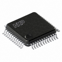
SC68C2550BIB48,151 NXP Semiconductors, SC68C2550BIB48,151 Datasheet - Page 19

SC68C2550BIB48,151
Manufacturer Part Number
SC68C2550BIB48,151
Description
IC UART DUAL W/FIFO 48-LQFP
Manufacturer
NXP Semiconductors
Type
5 V, 3.3 V and 2.5 V dual UART, 5 Mbit/s with 16-byte FIFOsr
Datasheet
1.SC68C2550BIB48151.pdf
(36 pages)
Specifications of SC68C2550BIB48,151
Number Of Channels
2, DUART
Package / Case
48-LQFP
Features
False-start Bit Detection
Fifo's
16 Byte
Voltage - Supply
2.5V, 3.3V, 5V
With Auto Flow Control
Yes
With False Start Bit Detection
Yes
With Modem Control
Yes
With Cmos
Yes
Mounting Type
Surface Mount
Data Rate
5 Mbps
Supply Voltage (max)
5.5 V
Supply Voltage (min)
2.25 V
Supply Current
4.5 mA
Maximum Operating Temperature
+ 85 C
Minimum Operating Temperature
- 40 C
Mounting Style
SMD/SMT
Operating Supply Voltage
2.5 V or 3.3 V or 5 V
Transmit Fifo
16Byte
Receive Fifo
16Byte
Transmitter And Receiver Fifo Counter
Yes
Package Type
LQFP
Operating Supply Voltage (max)
5.5V
Mounting
Surface Mount
Pin Count
48
Operating Temperature (min)
-40C
Operating Temperature (max)
85C
Operating Temperature Classification
Industrial
Lead Free Status / RoHS Status
Lead free / RoHS Compliant
Lead Free Status / RoHS Status
Lead free / RoHS Compliant, Lead free / RoHS Compliant
Other names
568-3296
935278765151
SC68C2550BIB48-S
935278765151
SC68C2550BIB48-S
Available stocks
Company
Part Number
Manufacturer
Quantity
Price
Company:
Part Number:
SC68C2550BIB48,151
Manufacturer:
NXP Semiconductors
Quantity:
10 000
NXP Semiconductors
SC68C2550B_3
Product data sheet
7.6 Modem Control Register (MCR)
This register controls the interface with the modem or a peripheral device.
Table 17.
Bit
7:5
4
3
2
1
0
Symbol
MCR[7:5]
MCR[4]
MCR[3]
MCR[2]
MCR[1]
MCR[0]
Modem Control Register bits description
5 V, 3.3 V and 2.5 V dual UART, 5 Mbit/s (max.), with 16-byte FIFOs
Description
reserved; set to ‘0’
Loopback. Enable the local Loopback mode (diagnostics). In this mode the
transmitter output (TXn) and the receiver input (RXn), CTSn, DSRn, CDn,
and RIn pins are disconnected from the SC68C2550B I/O pins. Internally
the modem data and control pins are connected into a loopback data
configuration (see
interrupts remain fully operational. The Modem Control Interrupts are also
operational, but the interrupts’ sources are switched to the lower four bits of
the Modem Control. Interrupts continue to be controlled by the IER
register.
OP2 control
(OP1). OP1A/OP1B are not available as an external signal in the
SC68C2550B. This bit is instead used in the Loopback mode only. In the
Loopback mode, this bit is used to write the state of the modem RIn
interface signal.
RTS
DTR
Rev. 03 — 9 October 2009
logic 0 = disable Loopback mode (normal default condition)
logic 1 = enable local Loopback mode (diagnostics)
logic 0 = forces OP2n output pin to HIGH state
logic 1 = forces OP2n output pin to LOW state. In Loopback mode,
controls MSR[7].
logic 0 = force RTSn output pin to a logic 1 (normal default condition)
logic 1 = force RTSn output pin to a logic 0
logic 0 = force DTRn output pin to a logic 1 (normal default condition)
logic 1 = force DTRn output pin to a logic 0
Figure
4). In this mode, the receiver and transmitter
SC68C2550B
© NXP B.V. 2009. All rights reserved.
19 of 36


