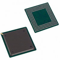
DS21Q55 Maxim Integrated Products, DS21Q55 Datasheet - Page 99

DS21Q55
Manufacturer Part Number
DS21Q55
Description
IC TXRX QUAD T1/E1/J1 SCT 256BGA
Manufacturer
Maxim Integrated Products
Datasheet
1.DS21Q55.pdf
(237 pages)
Specifications of DS21Q55
Function
Transceiver
Interface
E1, J1, T1
Number Of Circuits
4
Voltage - Supply
3.14 V ~ 3.47 V
Current - Supply
75mA
Operating Temperature
0°C ~ 70°C
Mounting Type
Surface Mount
Package / Case
256-BGA
Includes
BERT Generator and Detector, Dual HDLC Controllers
Lead Free Status / RoHS Status
Contains lead / RoHS non-compliant
Power (watts)
-
Available stocks
Company
Part Number
Manufacturer
Quantity
Price
Company:
Part Number:
DS21Q552
Manufacturer:
DALLAS
Quantity:
319
Company:
Part Number:
DS21Q552BN+
Manufacturer:
Maxim Integrated
Quantity:
10 000
Part Number:
DS21Q554
Manufacturer:
DALLAS
Quantity:
20 000
Part Number:
DS21Q554B+
Manufacturer:
MAXIM/美信
Quantity:
20 000
14.2.3 Software Signaling Insertion-Enable Registers, T1 Mode
In T1 mode, only registers SSIE1–SSIE3 are used since there are only 24 channels in a T1 frame.
Register Name:
Register Description:
Register Address:
Bit #
Name
Default
Bits 0 to 7/Software Signaling Insertion Enable for Channels 1 to 8 (CH1 to CH8). These bits determine which
channels are to have signaling inserted from the transmit signaling registers.
Register Name:
Register Description:
Register Address:
Bit #
Name
Default
Bits 0 to 7/Software Signaling Insertion Enable for Channels 9 to 16 (CH9 to CH16). These bits determine
which channels are to have signaling inserted from the transmit signaling registers.
Register Name:
Register Description:
Register Address:
Bit #
Name
Default
Bits 0 to 7/Software Signaling Insertion Enable for Channels 17 to 24 (CH17 to CH24). These bits determine
which channels are to have signaling inserted from the transmit signaling registers.
14.2.4 Hardware-Based Mode
In hardware-based mode, signaling data is input through the TSIG pin. This signaling PCM stream is
buffered and inserted to the data stream being input at the TSER pin.
Signaling data can be inserted on a per-channel basis by the transmit hardware-signaling channel-select
(THSCS) function. The user has the ability to control which channels are to have signaling data from the
TSIG pin inserted into them on a per-channel basis. See Section 4 for details on using this per-channel
(THSCS) feature. The signaling insertion capabilities of the framer are available whether the transmit-
side elastic store is enabled or disabled. If the elastic store is enabled, the backplane clock (TSYSCLK)
can be either 1.544MHz or 2.048MHz. Also, if the elastic is enabled in conjunction with transmit
hardware signaling, CCR3.7 must be set = 0.
0 = do not source signaling data from the TSx registers for this channel
1 = source signaling data from the TSx registers for this channel
0 = do not source signaling data from the TSx registers for this channel
1 = source signaling data from the TSx registers for this channel
0 = do not source signaling data from the TSx registers for this channel
1 = source signaling data from the TSx registers for this channel
CH16
CH24
CH8
7
0
7
0
7
0
CH15
CH23
CH7
SSIE1
Software Signaling Insertion Enable 1
08h
SSIE2
Software Signaling-Insertion Enable 2
09h
SSIE3
Software Signaling-Insertion Enable 3
0Ah
6
0
6
0
6
0
CH14
CH22
CH6
5
0
5
0
5
0
CH13
CH21
CH5
4
0
4
0
4
0
99 of 237
CH12
CH20
CH4
0
0
0
3
3
3
CH11
CH19
CH3
2
0
2
0
2
0
CH10
CH18
CH2
1
0
1
0
1
0
CH17
CH9
CH1
0
0
0
0
0
0


