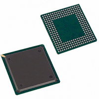
DS21Q55 Maxim Integrated Products, DS21Q55 Datasheet - Page 20

DS21Q55
Manufacturer Part Number
DS21Q55
Description
IC TXRX QUAD T1/E1/J1 SCT 256BGA
Manufacturer
Maxim Integrated Products
Datasheet
1.DS21Q55.pdf
(237 pages)
Specifications of DS21Q55
Function
Transceiver
Interface
E1, J1, T1
Number Of Circuits
4
Voltage - Supply
3.14 V ~ 3.47 V
Current - Supply
75mA
Operating Temperature
0°C ~ 70°C
Mounting Type
Surface Mount
Package / Case
256-BGA
Includes
BERT Generator and Detector, Dual HDLC Controllers
Lead Free Status / RoHS Status
Contains lead / RoHS non-compliant
Power (watts)
-
Available stocks
Company
Part Number
Manufacturer
Quantity
Price
Company:
Part Number:
DS21Q552
Manufacturer:
DALLAS
Quantity:
319
Company:
Part Number:
DS21Q552BN+
Manufacturer:
Maxim Integrated
Quantity:
10 000
Part Number:
DS21Q554
Manufacturer:
DALLAS
Quantity:
20 000
Part Number:
DS21Q554B+
Manufacturer:
MAXIM/美信
Quantity:
20 000
Signal Name:
Signal Description:
Signal Type:
Updated on the rising edge of TCLKO with the bipolar data out of the transmit-side formatter. Can be programmed
to source NRZ data by the output data format (IOCR1.0) control bit. This pin is normally connected to TPOSI.
Signal Name:
Signal Description:
Signal Type:
Updated on the rising edge of TCLKO with the bipolar data out of the transmit-side formatter. This pin is normally
connected to TNEGI.
Signal Name:
Signal Description:
Signal Type:
Buffered clock that is used to clock data through the transmit-side formatter (i.e., either TCLK or RCLKI). This pin
is normally connected to TCLKI.
Signal Name:
Signal Description:
Signal Type:
Sampled on the falling edge of TCLKI for data to be transmitted out onto the T1 line. Can be internally connected
to TPOSO by connecting the LIUC pin high. TPOSI and TNEGI can be connected together in NRZ applications.
Signal Name:
Signal Description:
Signal Type:
Sampled on the falling edge of TCLKI for data to be transmitted out onto the T1 line. Can be internally connected
to TNEGO by connecting the LIUC pin high. TPOSI and TNEGI can be connected together in NRZ applications.
Signal Name:
Signal Description:
Signal Type:
Line interface transmit clock. Can be internally connected to TCLKO by connecting the LIUC pin high.
TPOSOx
Transmit Positive-Data Output
Output
TNEGOx
Transmit Negative-Data Output
Output
TCLKOx
Transmit Clock Output
Output
TPOSIx
Transmit Positive-Data Input
Input
TNEGIx
Transmit Negative-Data Input
Input
TCLKIx
Transmit Clock Input
Input
20 of 237


