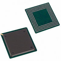
DS21Q55 Maxim Integrated Products, DS21Q55 Datasheet - Page 26

DS21Q55
Manufacturer Part Number
DS21Q55
Description
IC TXRX QUAD T1/E1/J1 SCT 256BGA
Manufacturer
Maxim Integrated Products
Datasheet
1.DS21Q55.pdf
(237 pages)
Specifications of DS21Q55
Function
Transceiver
Interface
E1, J1, T1
Number Of Circuits
4
Voltage - Supply
3.14 V ~ 3.47 V
Current - Supply
75mA
Operating Temperature
0°C ~ 70°C
Mounting Type
Surface Mount
Package / Case
256-BGA
Includes
BERT Generator and Detector, Dual HDLC Controllers
Lead Free Status / RoHS Status
Contains lead / RoHS non-compliant
Power (watts)
-
Available stocks
Company
Part Number
Manufacturer
Quantity
Price
Company:
Part Number:
DS21Q552
Manufacturer:
DALLAS
Quantity:
319
Company:
Part Number:
DS21Q552BN+
Manufacturer:
Maxim Integrated
Quantity:
10 000
Part Number:
DS21Q554
Manufacturer:
DALLAS
Quantity:
20 000
Part Number:
DS21Q554B+
Manufacturer:
MAXIM/美信
Quantity:
20 000
2.4 JTAG Test Access Port Pins
Signal Name:
Signal Description:
Signal Type:
JTRST is used to asynchronously reset the test access port controller. After power-up, JTRST must be toggled from
low to high. This action sets the device into the JTAG DEVICE ID mode. Normal device operation is restored by
pulling JTRST low. JTRST is pulled high internally by a 10kΩ resistor operation.
Signal Name:
Signal Description:
Signal Type:
This pin is sampled on the rising edge of JTCLK and is used to place the test access port into the various defined
IEEE 1149.1 states. This pin has a 10kΩ pullup resistor.
Signal Name:
Signal Description:
Signal Type:
This signal is used to shift data into JTDI on the rising edge and out of JTDO on the falling edge.
Signal Name:
Signal Description:
Signal Type:
Test instructions and data are clocked into this pin on the rising edge of JTCLK. This pin has a 10kΩ
pullup resistor.
Signal Name:
Signal Description:
Signal Type:
Test instructions and data are clocked out of this pin on the falling edge of JTCLK. If not used, this pin should be
left unconnected.
JTRST
IEEE 1149.1 Test Reset
Input
JTMS
IEEE 1149.1 Test Mode Select
Input
JTCLK
IEEE 1149.1 Test Clock Signal
Input
JTDI
IEEE 1149.1 Test Data Input
Input
JTDO
IEEE 1149.1 Test Data Output
Output
26 of 237


