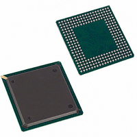
DS21Q55 Maxim Integrated Products, DS21Q55 Datasheet - Page 229

DS21Q55
Manufacturer Part Number
DS21Q55
Description
IC TXRX QUAD T1/E1/J1 SCT 256BGA
Manufacturer
Maxim Integrated Products
Datasheet
1.DS21Q55.pdf
(237 pages)
Specifications of DS21Q55
Function
Transceiver
Interface
E1, J1, T1
Number Of Circuits
4
Voltage - Supply
3.14 V ~ 3.47 V
Current - Supply
75mA
Operating Temperature
0°C ~ 70°C
Mounting Type
Surface Mount
Package / Case
256-BGA
Includes
BERT Generator and Detector, Dual HDLC Controllers
Lead Free Status / RoHS Status
Contains lead / RoHS non-compliant
Power (watts)
-
Available stocks
Company
Part Number
Manufacturer
Quantity
Price
Company:
Part Number:
DS21Q552
Manufacturer:
DALLAS
Quantity:
319
Company:
Part Number:
DS21Q552BN+
Manufacturer:
Maxim Integrated
Quantity:
10 000
Part Number:
DS21Q554
Manufacturer:
DALLAS
Quantity:
20 000
Part Number:
DS21Q554B+
Manufacturer:
MAXIM/美信
Quantity:
20 000
33.3 Receive-Side AC Characteristics
AC CHARACTERISTICS: RECEIVE SIDE
(Figure
(V
RCLKO Period
RCLKO Pulse Width
RCLKO Pulse Width
RCLKI Period
RCLKI Pulse Width
RSYSCLK Period
RSYSCLK Pulse Width
RSYNC Setup to RSYSCLK Falling
RSYNC Pulse Width
RPOSI/RNEGI Setup to RCLKI Falling
RPOSI/RNEGI Hold From RCLKI
Falling
RSYSCLK, RCLKI Rise and Fall Times
Delay RCLKO to RPOSO, RNEGO Valid
Delay RCLK to RSER, RSIG, RLINK
Valid
Delay RCLK to RCHCLK, RSYNC,
RCHBLK, RFSYNC, RLCLK
Delay RSYSCLK to RSER, RSIG Valid
Delay RSYSCLK to RCHCLK,
RCHBLK, RMSYNC, RSYNC
Note 1: Jitter attenuator enabled in the receive path.
Note 2: Jitter attenuator disabled or enabled in the transmit path.
Note 3: RSYSCLK = 1.544MHz
Note 4: RSYSCLK = 2.048MHz
Note 5: RSYSCLK = 4.096MHz
Note 6: RSYSCLK = 8.192MHz
Note 7: RSYSCLK = 16.384MHz
DD
= 3.3V ±5%, T
33-8,
PARAMETER
Figure
A
= 0°C to +70°C for DS21Q55; V
33-9, and
Figure
33-10)
SYMBOL
t
t
R
t
t
t
t
t
t
t
t
t
t
t
t
t
t
t
t
t
t
t
PW
HD
DD
LH
LH
CP
CH
CL
SH
SU
SU
D1
D2
D3
D4
LP
LL
LL
SP
SL
, t
F
229 of 237
DD
= 3.3V ±5%, T
(Note 1)
(Note 1)
(Note 2)
(Note 2)
(Note 3)
(Note 4)
(Note 5)
(Note 6)
(Note 7)
CONDITIONS
A
= -40°C to +85°C for DS21Q55N.)
MIN
200
200
150
150
20
20
20
20
20
50
20
20
488 (E1)
648 (T1)
488 (E1)
648 (T1)
0.5 t
0.5 t
0.5 t
0.5 t
0.5 t
0.5 t
0.5 t
0.5 t
TYP
648
488
244
122
61
CP
CP
LP
LP
LP
LP
SP
SP
MAX
22
50
50
50
22
22
UNITS
ns
ns
ns
ns
ns
ns
ns
ns
ns
ns
ns
ns
ns
ns
ns
ns
ns
ns
ns


