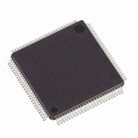
DS2156L+ Maxim Integrated Products, DS2156L+ Datasheet - Page 173

DS2156L+
Manufacturer Part Number
DS2156L+
Description
IC TXRX T1/E1/J1 1-CHIP 100-LQFP
Manufacturer
Maxim Integrated Products
Datasheet
1.DS2156L.pdf
(265 pages)
Specifications of DS2156L+
Function
Single-Chip Transceiver
Interface
E1, J1, T1, TDM, UTOPIA II
Number Of Circuits
1
Voltage - Supply
3.14 V ~ 3.47 V
Current - Supply
75mA
Operating Temperature
0°C ~ 70°C
Mounting Type
Surface Mount
Package / Case
100-LQFP
Includes
BERT Generator and Detector, CMI Coder and Decoder, HDLC Controller
Lead Free Status / RoHS Status
Lead free / RoHS Compliant
Power (watts)
-
- Current page: 173 of 265
- Download datasheet (2Mb)
The example in Figure 24-3 shows where the transmission of cells though the transmit interface is
stopped by the ATM, as no PHY is ready to accept cells. Polling continues. Several clock cycles later one
PHY gets ready to accept a cell. During the transmission pause, the UT-DATAx and UT-SOC can go into
high-impedance state as shown. UT-ENB is held in deasserted state. When a PHY is found that is ready to
accept a cell (PHY_N + 3 in this case), the address of this PHY must be applied again to select it. This is
necessary because of the 2-clock polling cycle, where the PHY is detected at the clock edge #15. At this
time, the address of PHY N + 3 is no longer on the bus and therefore must be applied again in the next
clock cycle. PHY N + 3 is selected with clock edge #16.
Figure 24-3. End and Restart of Cell at Transmit Interface
CELL XMIT TO:
UT-ADDRx
UT-DATAx
UT-CLAV
UT-ENB
UT-CLK
UT-SOC
1
N+1
P45
2
N+1
P46
PHY N
1F
3
P47
N
4
P48
N
1F
5
N+3
6
N+3
1F
POLLING
7
N+2
8
N+2
1F
173 of 265
9
N-1
10
N-1
1F
11
N
12
DETECTION
N
1F
13
N+3
14
SELECTION
N+3
1F
15
N+3
16
N+3
1F
H1
17
N-2
H2
18
PHY N+3
POLLING
N-2
1F
H3
19
N-3
H4
20
Related parts for DS2156L+
Image
Part Number
Description
Manufacturer
Datasheet
Request
R

Part Number:
Description:
Ds2156, Ds2156l, Ds2156ln T1/e1/j1 Single-chip Transceiver Tdm/utopia Ii Interface
Manufacturer:
Maxim Integrated Products, Inc.
Datasheet:

Part Number:
Description:
MAX7528KCWPMaxim Integrated Products [CMOS Dual 8-Bit Buffered Multiplying DACs]
Manufacturer:
Maxim Integrated Products
Datasheet:

Part Number:
Description:
Single +5V, fully integrated, 1.25Gbps laser diode driver.
Manufacturer:
Maxim Integrated Products
Datasheet:

Part Number:
Description:
Single +5V, fully integrated, 155Mbps laser diode driver.
Manufacturer:
Maxim Integrated Products
Datasheet:

Part Number:
Description:
VRD11/VRD10, K8 Rev F 2/3/4-Phase PWM Controllers with Integrated Dual MOSFET Drivers
Manufacturer:
Maxim Integrated Products
Datasheet:

Part Number:
Description:
Highly Integrated Level 2 SMBus Battery Chargers
Manufacturer:
Maxim Integrated Products
Datasheet:

Part Number:
Description:
Current Monitor and Accumulator with Integrated Sense Resistor; ; Temperature Range: -40°C to +85°C
Manufacturer:
Maxim Integrated Products

Part Number:
Description:
TSSOP 14/A�/RS-485 Transceivers with Integrated 100O/120O Termination Resis
Manufacturer:
Maxim Integrated Products

Part Number:
Description:
TSSOP 14/A�/RS-485 Transceivers with Integrated 100O/120O Termination Resis
Manufacturer:
Maxim Integrated Products

Part Number:
Description:
QFN 16/A�/AC-DC and DC-DC Peak-Current-Mode Converters with Integrated Step
Manufacturer:
Maxim Integrated Products

Part Number:
Description:
TDFN/A/65V, 1A, 600KHZ, SYNCHRONOUS STEP-DOWN REGULATOR WITH INTEGRATED SWI
Manufacturer:
Maxim Integrated Products

Part Number:
Description:
Integrated Temperature Controller f
Manufacturer:
Maxim Integrated Products

Part Number:
Description:
SOT23-6/I�/45MHz to 650MHz, Integrated IF VCOs with Differential Output
Manufacturer:
Maxim Integrated Products

Part Number:
Description:
SOT23-6/I�/45MHz to 650MHz, Integrated IF VCOs with Differential Output
Manufacturer:
Maxim Integrated Products

Part Number:
Description:
EVALUATION KIT/2.4GHZ TO 2.5GHZ 802.11G/B RF TRANSCEIVER WITH INTEGRATED PA
Manufacturer:
Maxim Integrated Products


