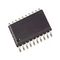
T5760NTGS Atmel, T5760NTGS Datasheet - Page 6

T5760NTGS
Manufacturer Part Number
T5760NTGS
Description
Manufacturer
Atmel
Datasheet
1.T5760NTGS.pdf
(38 pages)
Specifications of T5760NTGS
Operating Temperature (min)
-40C
Operating Temperature (max)
105C
Operating Temperature Classification
Industrial
Lead Free Status / Rohs Status
Not Compliant
4.3
6
FSK/ASK Demodulator and Data Filter
T5760/T5761
fcu_DF
Since different RF input networks may exhibit slightly different values for the LNA gain, the sen-
sitivity values given in the electrical characteristics refer to a specific input matching. This
matching is illustrated in
the same time power matching at RF_IN.
R
full sensitivity to reduced sensitivity or vice versa at any time. In polling mode, the receiver will
not wake up if the RF input signal does not exceed the selected sensitivity. If the receiver is
already active, the data stream at pin DATA will disappear when the input signal is lower than
defined by the reduced sensitivity. Instead of the data stream, the pattern according to
1
Figure 4-1.
The signal coming from the RSSI amplifier is converted into the raw data signal by the ASK/FSK
demodulator. The operating mode of the demodulator is set via the bit ASK/_FSK in the
OPMODE register. Logic L sets the demodulator to FSK, applying H to ASK mode.
In ASK mode an automatic threshold control circuit (ATC) is employed to set the detection refer-
ence voltage to a value where a good signal to noise ratio is achieved. This circuit also implies
the effective suppression of any kind of in-band noise signals or competing transmitters. If the
S/N (ratio to suppress in-band noise signals) exceeds about 10 dB the data signal can be
detected properly, but better values are found for many modulation schemes of the competing
transmitter.
The FSK demodulator is intended to be used for an FSK deviation of 10 kHz
FSK mode the data signal can be detected if the S/N (ratio to suppress in-band noise signals)
exceeds about 2 dB. This value is valid for all modulation schemes of a disturber signal.
The output signal of the demodulator is filtered by the data filter before it is fed into the digital
signal processing circuit. The data filter improves the S/N ratio as its passband can be adopted
to the characteristics of the data signal. The data filter consists of a 1
2
The highpass filter cut-off frequency is defined by an external capacitor connected to pin CDEM.
The cut-off frequency of the highpass filter is defined by the following formula:
In self-polling mode, the data filter must settle very rapidly to achieve a low current consumption.
Therefore, CDEM cannot be increased to very high values if self-polling is used. On the other
hand CDEM must be large enough to meet the data filter requirements according to the data sig-
nal. Recommended values for CDEM are given in the electrical characteristics.
nd
Sens
is issued at pin DATA to indicate that the receiver is still active (see
-order lowpass filter.
can be connected to V
=
------------------------------------------------------------ -
2
Steady L State Limited DATA Output Pattern
30 k
1
DATA
Figure 14-1 on page 29
CDEM
S
or GND via a microcontroller. The receiver can be switched from
t
DATA_min
t
DATA_L_max
and exhibits the best possible sensitivity and at
Figure 13-2 on page
st-
order high pass and a
f 100 kHz. In
4561C–RKE–05/05
Figure 4-
27).


