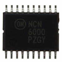
NCN6000DTBR2 ON Semiconductor, NCN6000DTBR2 Datasheet - Page 6

NCN6000DTBR2
Manufacturer Part Number
NCN6000DTBR2
Description
IC INTERFACE SMART CARD 20TSSOP
Manufacturer
ON Semiconductor
Datasheet
1.NCN6000DTBR2.pdf
(36 pages)
Specifications of NCN6000DTBR2
Applications
ATM Terminals, Gas Pumps, ISM
Interface
Microcontroller
Voltage - Supply
2.7 V ~ 6 V
Package / Case
20-TSSOP
Mounting Type
Surface Mount
Lead Free Status / RoHS Status
Contains lead / RoHS non-compliant
Other names
NCN6000DTBR2OSTR
Available stocks
Company
Part Number
Manufacturer
Quantity
Price
Part Number:
NCN6000DTBR2
Manufacturer:
ON/安森美
Quantity:
20 000
Part Number:
NCN6000DTBR2G
Manufacturer:
ON/安森美
Quantity:
20 000
ABBREVIATIONS
PIN FUNCTIONS AND DESCRIPTION
Pin
Lout_H
Lout_L
Cout
VCC
Icc
Class A
Class B
CS
Z
CRD_VCC
CRD_CLK
CRD_RST
CRD_IO
CRD_DET
ATR
PGM
INT
tr
tf
td
ts
1
2
3
4
5
6
7
PWR_ON
STATUS
RESET
Name
PGM
CS
A0
A1
DC−DC External Inductor
DC−DC External Inductor
Output Capacitor
Card Power Supply Input
Current at CRD_VCC Pin
5.0 V Smart Card
3.0 V Smart Card
Chip Select (from MPU)
High Impedance Logic State
Interface IC Card Power Supply Output
Interface IC Card Clock Output
Interface IC Card Reset Output
Interface IC Card I/O Signal Line
Interface IC Card Detection
Answer to Reset
Select Programming or Normal Operation
Interrupt (to MPU)
Rise Time
Fall Time
Delay Time
Storage Time
(according to ISO7816)
Pull Down
Pull Down
OUTPUT
Pull Up
INPUT
INPUT
INPUT
INPUT
INPUT
INPUT
Type
This pin is combined with A1, PGM, RESET and I/O to program the chip mode of operation
and to read the data provided by STATUS. (Figures 4 and 5 and Tables 2 and 3)
This pin is combined with A0, PGM, RESET and I/O to program the chip mode of operation
and to read the data provided by STATUS. (Figures 4 and 5 and Tables 2 and 3)
This pin is combined with A0, A1, RESET and I/O to program the chip mode of operation
and to read the data provided by STATUS. (Figures 4 and 5 and Tables 2 and 3)
This pin validates the operation of the internal DC−DC converter:
Note: The PWR_ON bit must be combined with a Low state CS signal to activate
the function. (Table 2)
This pin provides logic state related to the card and NCN6000 status. According to the A0,
A1 and PGM logic state, this pin carries either the Card present status or the Vbat or the
DC−DC operation state. When PGM = L, STATUS is not affected, see Table 2.
This pin provides the NCN6000 chip select function. The PWR_ON, RESET, I/O, A0, A1 and
PGM signals are disabled when CS = H. When PGM = L and CS = L, the device jumps to
the programming mode (Figure 4 and Tables 1, 2 and 3). The Chip Select pin must be a
unique physical address when more than one card are controlled by a single MPU. The data
presented by the MPU are latched upon positive going edge of the Chip Select pin.
This pin provides two modes of operation depending upon the logic state of PGM pin 3:
CS = L + PWR_ON = Negative going: DC−DC is OFF
CS = L + PWR_ON = Positive going: DC−DC is ON
PGM = 1: The signal present at this pin is translated to pin 12 (card reset
signal) when CS = L and PWR_ON = H. It is latched when CS = H.
PGM = 0: The signal present on this pin is used as a logic input to program the
internal functions (Figure 5 and Tables 2 and 3).
http://onsemi.com
NCN6000
6
Description


