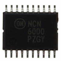
NCN6000DTBR2 ON Semiconductor, NCN6000DTBR2 Datasheet - Page 29

NCN6000DTBR2
Manufacturer Part Number
NCN6000DTBR2
Description
IC INTERFACE SMART CARD 20TSSOP
Manufacturer
ON Semiconductor
Datasheet
1.NCN6000DTBR2.pdf
(36 pages)
Specifications of NCN6000DTBR2
Applications
ATM Terminals, Gas Pumps, ISM
Interface
Microcontroller
Voltage - Supply
2.7 V ~ 6 V
Package / Case
20-TSSOP
Mounting Type
Surface Mount
Lead Free Status / RoHS Status
Contains lead / RoHS non-compliant
Other names
NCN6000DTBR2OSTR
Available stocks
Company
Part Number
Manufacturer
Quantity
Price
Part Number:
NCN6000DTBR2
Manufacturer:
ON/安森美
Quantity:
20 000
Part Number:
NCN6000DTBR2G
Manufacturer:
ON/安森美
Quantity:
20 000
Bidirectional Level Shifter
the MPU and the Smart Card I/O signals. When the start
sequence is completed, and if no failures have been detected,
the device becomes essentially transparent for the data
transferred on the I/O line. To fulfill the ISO7816−3
specification, both sides of the I/O line have built in pulsed
circuitry to accelerate the signal rise transient. The I/O line is
connected on both side of the interface by a NMOS switch
which provide the level shifter and, due to its relative high
internal impedance, protects the Smart Card in the event of
data collision. Such a situation could occurs if either the MPU
of the smart card forces a signal in the opposite logic level
direction.
any of the programming functions, the built in register holds
the previous state presents on the input I/O pin. This
The NCN6000 carries out the voltage difference between
When the CS signal goes High, or if the MPU is running
20 k
CARD ENABLE
V
I/O
bat
Figure 30. Basic Internal I/O Level Shifter
Seq 1
Q1
200 ns
LOGIC
Figure 32. Typical I/O and RST Signals During an ATR Sequence.
Q3
200 ns
Note: The I/O data depends solely upon the smart card ATR
content, the NCN6000 being not involved in these data.
Q2
GND
Q4
CRD_VCC = 3.0 V
CRD_VCC
20 k
CRD_IO
http://onsemi.com
NCN6000
29
mechanism is useful to force the CRD_IO card pin in either
a High or a Low pre−defined logic state. It is the responsibility
of the programmer to set up the I/O line according to the
system’s activity
CRD_IO line is deactivated. This mechanism avoids noise
presence on this line during any of the power operation.
externally connected device will be forward biased by the DC
current flowing through the pull up resistors as depicted in
Figure 30. Since these two resistors will carry 350 mA max
each under the worst case conditions, care must be observed
to make sure the external device will be capable to handle this
level of current. Note: the typical series impedance of the
internal MOS device (Q3, Figure 30) is 400 W.
when the stray capacitance is 15 pF.
Device Q4 provides a low impedance to ground when the
When either side of this level shifter is forced to Low, the
The oscillograms in Figure 31 give the worst case operation
CRD_VCC = 5.0 V
Figure 31. Typical CRD_IO Rise Time
CRD_VCC
I/O Card
Answer
Request Sends on
CRD_RST Line
NCN6000
Chip Select
CRD_IO
I/O


