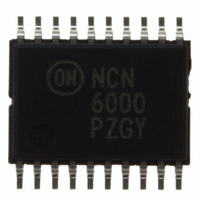
NCN6000DTBR2 ON Semiconductor, NCN6000DTBR2 Datasheet - Page 14

NCN6000DTBR2
Manufacturer Part Number
NCN6000DTBR2
Description
IC INTERFACE SMART CARD 20TSSOP
Manufacturer
ON Semiconductor
Datasheet
1.NCN6000DTBR2.pdf
(36 pages)
Specifications of NCN6000DTBR2
Applications
ATM Terminals, Gas Pumps, ISM
Interface
Microcontroller
Voltage - Supply
2.7 V ~ 6 V
Package / Case
20-TSSOP
Mounting Type
Surface Mount
Lead Free Status / RoHS Status
Contains lead / RoHS non-compliant
Other names
NCN6000DTBR2OSTR
Available stocks
Company
Part Number
Manufacturer
Quantity
Price
Part Number:
NCN6000DTBR2
Manufacturer:
ON/安森美
Quantity:
20 000
Part Number:
NCN6000DTBR2G
Manufacturer:
ON/安森美
Quantity:
20 000
DC−DC Converter and Card Detector Status
consult Figures 4 and 5 for a description of input and output
signals. The status message is described in Table 4.
condition, the Vbat OK message uses a negative logic as
depicted here below.
Table 4. Card and DC−DC Status Output
HIGH
HIGH
HIGH
HIGH
HIGH
HIGH
HIGH
HIGH
PGM
The NCN6000 status can be polled when CS = L. Please
Note: in order to cope with a start up under low battery
Typical CRD_VCC Rise Time @ Cout = 10 mF, V = 5.0 V
A1
H
H
H
H
L
L
L
L
A0
H
H
H
H
L
L
L
L
STATUS
HIGH
HIGH
HIGH
HIGH
LOW
LOW
LOW
LOW
Figure 6. Card Power Supply Turn ON and OFF Timing
No Card
Card Present
DC−DC Converter
DC−DC Converter OK
Vbat OK
Vbat Undervoltage
CRD_VCC OK
CRD_VCC Undervoltage
Overloaded
Message
http://onsemi.com
NCN6000
14
detection of the card, the state of the DC−DC converter, the
Vbat undervoltage and CRD_VCC undervoltage situations.
When PGM = H, the STATUS pin returns a High if a card is
detected present, a Low being asserted if there is no card
inserted. In any case, the external card is not automatically
powered up. When the external MPU asserts PWR_ON = H,
together with CS = L, the CRD_VCC supply is provided to
the card and the state of the DC−DC converter, the Vbat and
the CRD_VCC can be polled through the STATUS pin.
Card Power Supply Timing
depends upon the current capability of the DC−DC
converter associated with the external inductor L1 and the
reservoir capacitor connected across CRD_VCC and
GROUND.
depends upon the external reservoir capacitor and the peak
current absorbed by the internal CMOS transistor built
across CRD_VCC and GROUND. These behaviors are
depicted in Figure 6. Since these parameters have finite
values, depending upon the external constraints, the
designer must take care of these limits if the t
provided by the data sheets does not meet his requirements.
Typical CRD_VCC Fall Time @ Cout = 10 mF, V = 5.0 V
The STATUS pin provides a feedback related to the
At power up, the CRD_VCC power supply rise time
On the other hand, at turn off, the CRD_VCC fall time
ON
or the t
OFF


