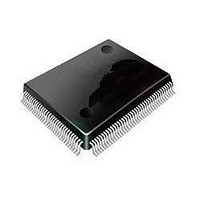
ST92F120V1Q7 STMicroelectronics, ST92F120V1Q7 Datasheet - Page 7

ST92F120V1Q7
Manufacturer Part Number
ST92F120V1Q7
Description
Microcontrollers (MCU) Flash 128K SPI/I2C
Manufacturer
STMicroelectronics
Datasheet
1.ST92F120V9Q7.pdf
(325 pages)
Specifications of ST92F120V1Q7
Data Bus Width
8 bit, 16 bit
Program Memory Type
Flash
Program Memory Size
128 KB
Data Ram Size
4 KB
Interface Type
I2C, SPI
Maximum Clock Frequency
24 MHz
Number Of Programmable I/os
77
Number Of Timers
5
Maximum Operating Temperature
+ 105 C
Mounting Style
SMD/SMT
Package / Case
PQFP-100
Minimum Operating Temperature
- 40 C
On-chip Adc
8 bit, 16 Channel
Lead Free Status / Rohs Status
No
Available stocks
Company
Part Number
Manufacturer
Quantity
Price
Company:
Part Number:
ST92F120V1Q7
Manufacturer:
ST
Quantity:
6 765
Part Number:
ST92F120V1Q7
Manufacturer:
ST
Quantity:
20 000
Part Number:
ST92F120V1Q7C
Manufacturer:
ST
Quantity:
20 000
Company:
Part Number:
ST92F120V1Q7DTR
Manufacturer:
MAXIM
Quantity:
2 854
- Current page: 7 of 325
- Download datasheet (3Mb)
Figure 2. CMOS Basic Inverter
When an input is kept at logic zero, the N-channel
transistor is off, while the P-channel is on and can
conduct. The opposite occurs when an input is
kept at logic one. CMOS transistors are essentially
linear devices with relatively broad switching
points. During commutation, the input passes
through midsupply, and there is a region of input
voltage values where both P and N-channel tran-
sistors are on. Since normally the transitions are
fast, there is a very short time in which a current
can flow: once the switching is completed there is
no longer current. This phenomenon explains why
the overall current depends on the switching rate:
the consumption is directly proportional to the
number of transistors inside the device which are
in the linear region during transitions, charging and
discharging internal capacitances.
In order to avoid extra power supply current, it is
important to bias input pins properly when not
used. In fact, if the input impedance is very high,
pins can float, when not connected, either to a
midsupply level or can oscillate (injecting noise in
the device).
Depending on the specific configuration of each
I/O pin on different ST9 devices, it can be more or
less critical to leave unused pins floating. For this
reason, on most pins, the configuration after RE-
SET enables an internal weak pull-up transistor in
order to avoid floating conditions. For other pins
this is intrinsically forbidden, like for the true open-
drain pins. In any case, the application software
must program the right state for unused pins to
avoid conflicts with external circuitry (whichever it
is: pull-up, pull-down, floating, etc.).
The suggested method of terminating unused I/O
is to connect an external individual pull-up or pull-
down for each pin, even though initialization soft-
ware can force outputs to a specified and defined
OUT
P
N
V
V
DD
SS
IN
value, during a particular phase of the RESET rou-
tine there could be an undetermined status at the
input section.
Usage of pull-ups and/or pull-downs is preferable
in place of direct connection to V
up or pull-down resistors are used, inputs can be
forced for test purposes to a different value, and
outputs can be programmed to both digital levels
without generating high current drain due to the
conflict.
Anyway, during system verification flow, attention
must be paid to reviewing the connection of each
pin, in order to avoid potential problems.
1.2.4 Avoidance of Pin Damage
Although integrated circuit data sheets provide the
user with conservative limits and conditions in or-
der to prevent damage, sometimes it is useful for
the hardware system designer to know the internal
failure mechanisms: the risk of exposure to illegal
voltages and conditions can be reduced by smart
protection design.
It is not possible to classify and to predict all the
possible damage resulting from violating maxi-
mum ratings and conditions, due to the large
number of variables that come into play in defining
the failures: in fact, when an overvoltage condition
is applied, the effects on the device can vary sig-
nificantly depending on lot-to-lot process varia-
tions, operating temperature, external interfacing
of the ST9 with other devices, etc.
In the following sections, background technical in-
formation is given in order to help system design-
ers to reduce risk of damage to the ST9 device.
1.2.4.1 Electrostatic Discharge and Latchup
CMOS integrated circuits are generally sensitive
to exposure to high voltage static electricity, which
can induce permanent damage to the device: a
typical failure is the breakdown of thin oxides,
which causes high leakage current and sometimes
shorts.
Latchup is another typical phenomenon occurring
in integrated circuits: unwanted turning on of para-
sitic bipolar structures, or silicon-controlled rectifi-
ers (SCR), may overheat and rapidly destroy the
device. These unintentional structures are com-
posed of P and N regions which work as emitters,
bases and collectors of parasitic bipolar transis-
tors: the bulk resistance of the silicon in the wells
and substrate act as resistors on the SCR struc-
ture. Applying voltages below V
and when the level of current is able to generate a
ST92F120 - GENERAL DESCRIPTION
SS
DD
or above V
or V
SS
. If pull-
7/324
DD
9
,
Related parts for ST92F120V1Q7
Image
Part Number
Description
Manufacturer
Datasheet
Request
R

Part Number:
Description:
8/16-bit Flash Mcu Family With Ram, Eeprom And J1850 Blpd
Manufacturer:
STMicroelectronics
Datasheet:

Part Number:
Description:
STMicroelectronics [RIPPLE-CARRY BINARY COUNTER/DIVIDERS]
Manufacturer:
STMicroelectronics
Datasheet:

Part Number:
Description:
STMicroelectronics [LIQUID-CRYSTAL DISPLAY DRIVERS]
Manufacturer:
STMicroelectronics
Datasheet:

Part Number:
Description:
BOARD EVAL FOR MEMS SENSORS
Manufacturer:
STMicroelectronics
Datasheet:

Part Number:
Description:
NPN TRANSISTOR POWER MODULE
Manufacturer:
STMicroelectronics
Datasheet:

Part Number:
Description:
TURBOSWITCH ULTRA-FAST HIGH VOLTAGE DIODE
Manufacturer:
STMicroelectronics
Datasheet:

Part Number:
Description:
Manufacturer:
STMicroelectronics
Datasheet:

Part Number:
Description:
DIODE / SCR MODULE
Manufacturer:
STMicroelectronics
Datasheet:

Part Number:
Description:
DIODE / SCR MODULE
Manufacturer:
STMicroelectronics
Datasheet:

Part Number:
Description:
Search -----> STE16N100
Manufacturer:
STMicroelectronics
Datasheet:

Part Number:
Description:
Search ---> STE53NA50
Manufacturer:
STMicroelectronics
Datasheet:

Part Number:
Description:
NPN Transistor Power Module
Manufacturer:
STMicroelectronics
Datasheet:


