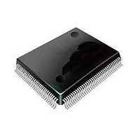
ST92F120V1Q7 STMicroelectronics, ST92F120V1Q7 Datasheet - Page 296

ST92F120V1Q7
Manufacturer Part Number
ST92F120V1Q7
Description
Microcontrollers (MCU) Flash 128K SPI/I2C
Manufacturer
STMicroelectronics
Datasheet
1.ST92F120V9Q7.pdf
(325 pages)
Specifications of ST92F120V1Q7
Data Bus Width
8 bit, 16 bit
Program Memory Type
Flash
Program Memory Size
128 KB
Data Ram Size
4 KB
Interface Type
I2C, SPI
Maximum Clock Frequency
24 MHz
Number Of Programmable I/os
77
Number Of Timers
5
Maximum Operating Temperature
+ 105 C
Mounting Style
SMD/SMT
Package / Case
PQFP-100
Minimum Operating Temperature
- 40 C
On-chip Adc
8 bit, 16 Channel
Lead Free Status / Rohs Status
No
Available stocks
Company
Part Number
Manufacturer
Quantity
Price
Company:
Part Number:
ST92F120V1Q7
Manufacturer:
ST
Quantity:
6 765
Part Number:
ST92F120V1Q7
Manufacturer:
ST
Quantity:
20 000
Part Number:
ST92F120V1Q7C
Manufacturer:
ST
Quantity:
20 000
Company:
Part Number:
ST92F120V1Q7DTR
Manufacturer:
MAXIM
Quantity:
2 854
- Current page: 296 of 325
- Download datasheet (3Mb)
ST92F120 - ELECTRICAL CHARACTERISTICS
EXTERNAL BUS TIMING TABLE
(V
Note: The value in the left hand column shows the formula used to calculate the timing minimum or maximum from the oscillator clock period,
prescaler value and number of wait cycles inserted.
The values in the right hand two columns show the timing minimum and maximum for an external clock at 24MHz, prescaler value of zero
and zero wait states.
Legend:
Tck = INTCLK period = OSCIN period when OSCIN is not divided by 2;
TckH = INTCLK high pulse width (normally = Tck/2, except when INTCLK = OSCIN, in which case it is OSCIN high pulse width)
TckL = INTCLK low pulse width (normally = Tck/2, except when INTCLK = OSCIN, in which case it is OSCIN low pulse width)
P = clock prescaling value (=PRS; division factor = 1+P)
Wa = wait cycles on
Wd = wait cycles on
296/324
1
N°
10 TdDS (AS)
11 TsR/W (AS)
12 TdDSR (R/W)
13 TdDW (DSW)
14 TsD(DSW)
15 ThDS (DW)
16 TdA (DR)
17 TdAs (DS)
1
2
3
4
5
6
7
8
9
DD
TsA (AS)
ThAS (A)
TdAS (DR)
TwAS
TdAz (DS)
TwDS
TdDSR (DR)
ThDR (DS)
TdDS (A)
= 5V
Symbol
10%, T
AS
DS
2 x OSCIN period when OSCIN is divided by 2;
OSCIN period x PLL factor when the PLL is enabled.
; = max (P, programmed wait cycles in EMR2, requested wait cycles with
; = max (P, programmed wait cycles in WCR, requested wait cycles with
A
Address Set-up Time before AS
Address Hold Time after AS
AS
AS Low Pulse Width
Address Float to DS
DS Low Pulse Width
DS
Data to DS
DS
DS
RW Set-up Time before AS
DS
Write Data Valid to DS
Write Data Set-up before DS
Data Hold Time after DS
Address Valid to Data Valid Delay (read)
AS
=
–
40°C to +105°C, C
to Data Available (read)
to DS
to Data Valid Delay (read)
to Address Active Delay
to AS
to RW and Address Not Valid Delay
Hold Time (read)
Delay
Delay
Parameter
Load
Delay
(write)
= 50pF, f
INTCLK
Tck x Wa+TckH-9
TckL-4
Tck x (Wd+1)+3
Tck x Wa+TckH-5
0
Tck x Wd+TckH-5
Tck x Wd+TckH+4
7
TckL+11
TckL-4
Tck x Wa+TckH-17
TckL-1
-16
Tck x Wd+TckH-16
TckL-3
Tck x (Wa+Wd+1)+TckH-7
TckL-6
= 24MHz, unless otherwise specified)
Formula
WAIT
WAIT
Value (Note)
)
)
Min Max
-16
12
17
16
16
32
17
20
18
15
0
7
4
5
45
25
55
Unit
ns
ns
ns
ns
ns
ns
ns
ns
ns
ns
ns
ns
ns
ns
ns
ns
ns
Related parts for ST92F120V1Q7
Image
Part Number
Description
Manufacturer
Datasheet
Request
R

Part Number:
Description:
8/16-bit Flash Mcu Family With Ram, Eeprom And J1850 Blpd
Manufacturer:
STMicroelectronics
Datasheet:

Part Number:
Description:
STMicroelectronics [RIPPLE-CARRY BINARY COUNTER/DIVIDERS]
Manufacturer:
STMicroelectronics
Datasheet:

Part Number:
Description:
STMicroelectronics [LIQUID-CRYSTAL DISPLAY DRIVERS]
Manufacturer:
STMicroelectronics
Datasheet:

Part Number:
Description:
BOARD EVAL FOR MEMS SENSORS
Manufacturer:
STMicroelectronics
Datasheet:

Part Number:
Description:
NPN TRANSISTOR POWER MODULE
Manufacturer:
STMicroelectronics
Datasheet:

Part Number:
Description:
TURBOSWITCH ULTRA-FAST HIGH VOLTAGE DIODE
Manufacturer:
STMicroelectronics
Datasheet:

Part Number:
Description:
Manufacturer:
STMicroelectronics
Datasheet:

Part Number:
Description:
DIODE / SCR MODULE
Manufacturer:
STMicroelectronics
Datasheet:

Part Number:
Description:
DIODE / SCR MODULE
Manufacturer:
STMicroelectronics
Datasheet:

Part Number:
Description:
Search -----> STE16N100
Manufacturer:
STMicroelectronics
Datasheet:

Part Number:
Description:
Search ---> STE53NA50
Manufacturer:
STMicroelectronics
Datasheet:

Part Number:
Description:
NPN Transistor Power Module
Manufacturer:
STMicroelectronics
Datasheet:


