DS3154+ Maxim Integrated Products, DS3154+ Datasheet - Page 4
DS3154+
Manufacturer Part Number
DS3154+
Description
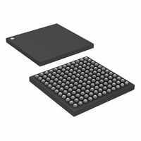
IC LIU DS3/E3/STS1 QUAD 144CSBGA
Manufacturer
Maxim Integrated Products
Type
Line Interface Units (LIUs)r
Datasheet
1.DS3151.pdf
(61 pages)
Specifications of DS3154+
Number Of Drivers/receivers
4/4
Protocol
IEEE 1149.1
Voltage - Supply
3.135 V ~ 3.465 V
Mounting Type
Surface Mount
Package / Case
144-CSBGA
Lead Free Status / RoHS Status
Lead free / RoHS Compliant


DS3151/DS3152/DS3153/DS3154 Single/Dual/Triple/Quad DS3/E3/STS-1 LIUs
LIST OF TABLES
Table 1-A. Applicable Telecommunications Standards ..............................................................................6
Table 4-A. Active I/O Pins—Hardware and CPU Bus Modes...................................................................10
Table 4-B. Transmitter Pin Descriptions ...................................................................................................11
Table 4-C. Receiver Pin Descriptions.......................................................................................................12
Table 4-D. Global Pin Descriptions ..........................................................................................................13
Table 4-E. JTAG and Test Pin Descriptions .............................................................................................14
Table 4-F. Transmitter Data Select Options .............................................................................................14
Table 4-G. Receiver PRBS Pattern Select Options..................................................................................14
Table 5-A. Register Map...........................................................................................................................15
Table 7-A. DS3 Waveform Template........................................................................................................26
Table 7-B. DS3 Waveform Test Parameters and Limits...........................................................................26
Table 7-C. STS-1 Waveform Template ....................................................................................................26
Table 7-D. STS-1 Waveform Test Parameters and Limits .......................................................................27
Table 7-E. E3 Waveform Test Parameters and Limits .............................................................................27
Table 11-A. Transformer Characteristics..................................................................................................31
Table 11-B. Recommended Transformers ...............................................................................................31
Table 12-A. JTAG Instruction Codes ........................................................................................................35
Table 12-B. JTAG ID Code.......................................................................................................................35
Table 13-A. Recommended DC Operating Conditions.............................................................................37
Table 13-B. DC Characteristics ................................................................................................................37
Table 13-C. Framer Interface Timing .......................................................................................................38
Table 13-D. Receiver Input Characteristics—DS3 and STS-1 Modes .....................................................39
Table 13-E. Receiver Input Characteristics—E3 Mode ............................................................................39
Table 13-F. Transmitter Output Characteristics—DS3 and STS-1 Modes ...............................................40
Table 13-G. Transmitter Output Characteristics—E3 Mode .....................................................................40
Table 13-H. CPU Bus Timing ...................................................................................................................40
Table 13-I. JTAG Interface Timing ...........................................................................................................45
Table 14-A. Pin Assignments Sorted by Signal Name .............................................................................46
Table 14-B. Pin Assignments Sorted by Pin Number ...............................................................................48
Table 16-A. Thermal Properties, Natural Convection ...............................................................................60
Table 16-B. Theta-JA (θ
) vs. Airflow ......................................................................................................60
JA
4 of 61
Related parts for DS3154+
Image
Part Number
Description
Manufacturer
Datasheet
Request
R

Part Number:
Description:
MAX7528KCWPMaxim Integrated Products [CMOS Dual 8-Bit Buffered Multiplying DACs]
Manufacturer:
Maxim Integrated Products
Datasheet:
Part Number:
Description:
Single +5V, fully integrated, 1.25Gbps laser diode driver.
Manufacturer:
Maxim Integrated Products
Datasheet:
Part Number:
Description:
Single +5V, fully integrated, 155Mbps laser diode driver.
Manufacturer:
Maxim Integrated Products
Datasheet:
Part Number:
Description:
VRD11/VRD10, K8 Rev F 2/3/4-Phase PWM Controllers with Integrated Dual MOSFET Drivers
Manufacturer:
Maxim Integrated Products
Datasheet:
Part Number:
Description:
Highly Integrated Level 2 SMBus Battery Chargers
Manufacturer:
Maxim Integrated Products
Datasheet:
Part Number:
Description:
Current Monitor and Accumulator with Integrated Sense Resistor; ; Temperature Range: -40°C to +85°C
Manufacturer:
Maxim Integrated Products
Part Number:
Description:
TSSOP 14/A�/RS-485 Transceivers with Integrated 100O/120O Termination Resis
Manufacturer:
Maxim Integrated Products
Part Number:
Description:
TSSOP 14/A�/RS-485 Transceivers with Integrated 100O/120O Termination Resis
Manufacturer:
Maxim Integrated Products
Part Number:
Description:
QFN 16/A�/AC-DC and DC-DC Peak-Current-Mode Converters with Integrated Step
Manufacturer:
Maxim Integrated Products
Part Number:
Description:
TDFN/A/65V, 1A, 600KHZ, SYNCHRONOUS STEP-DOWN REGULATOR WITH INTEGRATED SWI
Manufacturer:
Maxim Integrated Products
Part Number:
Description:
Integrated Temperature Controller f
Manufacturer:
Maxim Integrated Products
Part Number:
Description:
SOT23-6/I�/45MHz to 650MHz, Integrated IF VCOs with Differential Output
Manufacturer:
Maxim Integrated Products
Part Number:
Description:
SOT23-6/I�/45MHz to 650MHz, Integrated IF VCOs with Differential Output
Manufacturer:
Maxim Integrated Products
Part Number:
Description:
EVALUATION KIT/2.4GHZ TO 2.5GHZ 802.11G/B RF TRANSCEIVER WITH INTEGRATED PA
Manufacturer:
Maxim Integrated Products
Part Number:
Description:
QFN/E/DUAL PCIE/SATA HIGH SPEED SWITCH WITH INTEGRATED BIAS RESISTOR
Manufacturer:
Maxim Integrated Products
Datasheet: