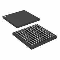
DS3154+ Maxim Integrated Products, DS3154+ Datasheet - Page 25

DS3154+
Manufacturer Part Number
DS3154+
Description
IC LIU DS3/E3/STS1 QUAD 144CSBGA
Manufacturer
Maxim Integrated Products
Type
Line Interface Units (LIUs)r
Datasheet
1.DS3151.pdf
(61 pages)
Specifications of DS3154+
Number Of Drivers/receivers
4/4
Protocol
IEEE 1149.1
Voltage - Supply
3.135 V ~ 3.465 V
Mounting Type
Surface Mount
Package / Case
144-CSBGA
Lead Free Status / RoHS Status
Lead free / RoHS Compliant
DS3151/DS3152/DS3153/DS3154 Single/Dual/Triple/Quad DS3/E3/STS-1 LIUs
7. TRANSMITTER
Transmit Clock. The clock applied at the TCLK input clocks in data on the TPOS/TDAT and TNEG pins. If the jitter
attenuator is not enabled in the transmit path, the signal on TCLK is the transmit line clock and must be
transmission quality (i.e., ±20ppm frequency accuracy and low jitter). If the jitter attenuator is enabled in the
transmit path, the signal on TCLK can be jittery and/or periodically gapped (not exceeding 8UI), but must still have
an average frequency within ±20ppm of the nominal line rate. When enabled in the transmit path, the jitter
attenuator generates the transmit line clock from the signal applied on the appropriate MCLK pin. The signal on the
MCLK pin must, therefore, be a transmission-quality clock (±20ppm frequency accuracy and low jitter).
The polarity of TCLK can be inverted to support glueless interfacing to a variety of neighboring components.
Normally data is sampled on the TPOS/TDAT and TNEG pins on the rising edge of TCLK. To sample data on the
falling edge of TCLK, pull the TCINV pin high (hardware mode) or set the TCINV configuration bit (CPU bus mode).
Framer Interface Format and the B3ZS/HDB3 Encoder. Data to be transmitted can be input in either binary or
bipolar format. To select the binary interface format, pull the TBIN pin high (hardware mode) or set the TBIN
configuration bit (CPU bus mode). In binary format, the B3ZS/HBD3 encoder is enabled, and the data to be
transmitted is sampled on the TDAT pin. The TNEG pin is ignored in binary interface mode and should be wired
low. In DS3 and STS-1 modes, the B3ZS/HDB3 encoder operates in the B3ZS mode. In E3 mode the encoder
operates in HDB3 mode.
To select the bipolar interface format, pull the TBIN pin low (hardware mode) or clear the TBIN configuration bit
(CPU bus mode). In bipolar format, the B3ZS/HDB3 encoder is disabled and the data to be transmitted is sampled
on the TPOS and TNEG pins. Positive-polarity pulses are indicated by TPOS = 1, while negative-polarity pulses
are indicated by TNEG = 1.
Pattern Generation. The transmitter can generate several patterns internally, including unframed all ones (E3
AIS), 100100…, and DS3 AIS. See
Figure 7-2
for the structure of the DS3 AIS signal. The TDSA and TDSB input
pins (hardware mode) or the TDSA and TDSB control bits (CPU bus mode) are used to select these patterns.
Table 4-F
indicates the possible selections.
Waveshaping, Line Build-Out, Line Driver. The waveshaping block converts the transmit clock, positive data,
and negative data signals into a single AMI signal with the waveshape required for interfacing to DS3/E3/STS-1
lines.
Table 7-A
through
Table 7-E
and
Figure 7-1
show the waveform template specifications and test parameters.
Because DS3 and STS-1 signals must meet the waveform templates at the cross-connect through any cable length
from 0 to 450ft, the waveshaping circuitry includes a selectable LBO feature. For cable lengths of 225ft or greater,
the TLBO pin (hardware mode) or the TLBO configuration bit (CPU bus mode) should be low. When TLBO is low,
output pulses are driven onto the coaxial cable without any preattenuation. For cable lengths less than 225ft, TLBO
should be high to enable the LBO circuitry. When TLBO is high, pulses are preattenuated by the LBO circuitry
before being driven onto the coaxial cable. The LBO circuitry provides attenuation that mimics the attenuation of
225ft of coaxial cable.
The transmitter line driver can be disabled and the TXP and TXN outputs tri-stated by asserting the TTS input or
the TTS configuration bit. Powering down the transmitter through the TPD configuration bit (CPU bus mode) also
tri-states the TXP and TXN outputs.
Interfacing to the Line. The transmitter interfaces to the outgoing DS3/E3/STS-1 coaxial cable (75Ω) through a
2:1 step-down transformer connected to the TXP and TXN pins.
Figure 1-1
shows the arrangement of the
transformer and other recommended interface components.
Table 11-A
specifies the required characteristics of the
transformer.
Transmit Driver Monitor. If the transmit driver monitor detects a faulty transmitter, it activates the TDM output
(hardware mode or CPU bus mode) or sets the TDM status bit and optionally activates the INT output (CPU bus
mode). When the transmitter is tri-stated, the transmit driver monitor is also disabled. The transmitter is declared to
be faulty when the transmitter outputs see a load of less than ~25Ω.
25 of 61


