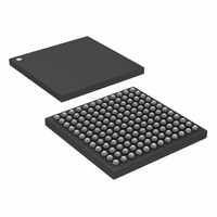
DS3154+ Maxim Integrated Products, DS3154+ Datasheet - Page 35

DS3154+
Manufacturer Part Number
DS3154+
Description
IC LIU DS3/E3/STS1 QUAD 144CSBGA
Manufacturer
Maxim Integrated Products
Type
Line Interface Units (LIUs)r
Datasheet
1.DS3151.pdf
(61 pages)
Specifications of DS3154+
Number Of Drivers/receivers
4/4
Protocol
IEEE 1149.1
Voltage - Supply
3.135 V ~ 3.465 V
Mounting Type
Surface Mount
Package / Case
144-CSBGA
Lead Free Status / RoHS Status
Lead free / RoHS Compliant
12.3
The instruction register contains a shift register as well as a latched parallel output and is 3 bits in length. When the
TAP controller enters the Shift-IR state, the instruction shift register is connected between JTDI and JTDO. While in
the Shift-IR state, a rising edge on JTCLK with JTMS low shifts data one stage toward the serial output at JTDO. A
rising edge on JTCLK in the Exit1-IR state or the Exit2-IR state with JTMS high moves the controller to the Update-
IR state. The falling edge of that same JTCLK latches the data in the instruction shift register to the instruction
parallel output.
codes.
Table 12-A. JTAG Instruction Codes
SAMPLE/PRELOAD. SAMPLE/RELOAD is a mandatory instruction for the IEEE 1149.1 specification. This
instruction supports two functions. The digital I/Os of the device can be sampled at the boundary scan register
without interfering with the device’s normal operation by using the Capture-DR state. SAMPLE/PRELOAD also
allows the DS315x to shift data into the boundary scan register through JTDI using the Shift-DR state.
EXTEST. EXTEST allows testing of the interconnections to the device. When the EXTEST instruction is latched in
the instruction register, the following actions occur. Once enabled through the Update-IR state, the parallel outputs
of the digital output pins are driven. The boundary scan register is connected between JTDI and JTDO. The
Capture-DR samples all digital inputs into the boundary scan register.
BYPASS. When the BYPASS instruction is latched into the parallel instruction register, JTDI connects to JTDO
through the 1-bit bypass test register. This allows data to pass from JTDI to JTDO without affecting the device’s
normal operation.
IDCODE. When the IDCODE instruction is latched into the parallel instruction register, the identification test
register is selected. The device identification code is loaded into the identification register on the rising edge of
JTCLK, following entry into the Capture-DR state. Shift-DR can be used to shift the identification code out serially
through JTDO. During Test-Logic-Reset, the identification code is forced into the instruction register’s parallel
output.
HIGHZ. All digital outputs are placed into a high-impedance state. The bypass register is connected between JTDI
and JTDO.
CLAMP. All digital output pins output data from the boundary scan parallel output while connecting the bypass
register between JTDI and JTDO. The outputs do not change during the CLAMP instruction.
Table 12-B. JTAG ID Code
DS3154
DS3153
DS3152
DS3151
SAMPLE/PRELOAD
PART
INSTRUCTIONS
JTAG Instruction Register and Instructions
BYPASS
EXTEST
IDCODE
CLAMP
HIGHZ
Table 12-A
Consult factory
Consult factory
Consult factory
Consult factory
REVISION
shows the instructions supported by the DS315x and their respective operational binary
SELECTED REGISTER
Device Identification
Boundary Scan
Boundary Scan
0000000000110011
0000000000110010
0000000000110000
0000000000100000
DS3151/DS3152/DS3153/DS3154 Single/Dual/Triple/Quad DS3/E3/STS-1 LIUs
Bypass
Bypass
Bypass
DEVICE CODE
35 of 61
INSTRUCTION CODES
MANUFACTURER CODE
00010100001
00010100001
00010100001
00010100001
010
111
000
011
100
001
REQUIRED
1
1
1
1


