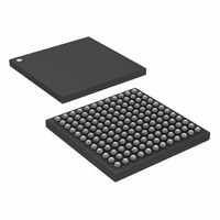
DS3154+ Maxim Integrated Products, DS3154+ Datasheet - Page 29

DS3154+
Manufacturer Part Number
DS3154+
Description
IC LIU DS3/E3/STS1 QUAD 144CSBGA
Manufacturer
Maxim Integrated Products
Type
Line Interface Units (LIUs)r
Datasheet
1.DS3151.pdf
(61 pages)
Specifications of DS3154+
Number Of Drivers/receivers
4/4
Protocol
IEEE 1149.1
Voltage - Supply
3.135 V ~ 3.465 V
Mounting Type
Surface Mount
Package / Case
144-CSBGA
Lead Free Status / RoHS Status
Lead free / RoHS Compliant
Loopbacks. Each LIU has three internal loopbacks. See
(hardware mode) or LLB and RLB control bits (CPU bus mode) enable these loopbacks. When LLB = RLB = 0,
loopbacks are disabled. Setting RLB = 1 with LLB = 0 enables remote loopback, which loops recovered clock and
data back through the LIU transmitter. During remote loopback, recovered clock and data are output on RCLK,
RPOS/RDAT, and RNEG/RLCV, but the TPOS/TDAT and TNEG pins are ignored. Setting LLB = 1 with RLB = 0
enables analog local loopback, which loops the outgoing transmit signal back to the receiver’s analog front end.
Setting LLB = RLB = 1 enables digital local loopback, which loops digital transmit clock and data back to the
receiver’s digital circuitry, including the LOS detector, the B3ZS/HDB3 decoder, and the PRBS detector. When
either of the local loopbacks is enabled, the transmit signal is output normally on TXP/TXN, but the received signal
on RXP/RXN is ignored.
Figure 8-1. PRBS Output with Normal RCLK Operation
Figure 8-2. PRBS Output with Inverted RCLK Operation
9. JITTER ATTENUATOR
Each LIU contains an on-board jitter attenuator that can be placed in the receive path or the transmit path or can
be disabled. The TJA and RJA pins (hardware mode) or the TJA and RJA control bits (CPU bus mode) specify how
the jitter attenuator is used. Setting TJA = RJA = 0 disables the jitter attenuator. To use the jitter attenuator in the
receive path, set RJA = 1 (with TJA = 0). To use it in the transmit path, set TJA = 1.
jitter attenuation for the device when the jitter attenuator is enabled.
when the jitter attenuator is disabled.
The jitter attenuator consists of a narrowband PLL to retime the selected clock, a 16 x 2-bit FIFO to buffer the
associated data while the clock is being retimed, and logic to prevent FIFO over/underflow in the presence of very
large jitter amplitudes.
The jitter attenuator requires a transmission-quality master clock (i.e., ±20ppm frequency accuracy and low jitter).
When enabled in the receive path, the JA can obtain its master clock from the appropriate MCLK pin or the TCLK
pin. If the signal on the MCLK pin is toggling, the JA uses the signal on the MCLK pin as its master clock. If the
MCLK pin is high, the JA uses the signal on the TCLK pin as its master clock. When enabled in the transmit path,
PRBS
RCLK
PRBS
RCLK
PRBS DETECTOR
PRBS DETECTOR
IS NOT IN SYNC
IS NOT IN SYNC
PRBS PIN PULSES HIGH FOR EACH BIT
PRBS PIN PULSES HIGH FOR EACH BIT
RCINV = 0
RCINV = 1
PRBS DETECTOR IS IN SYNC; THE
PRBS DETECTOR IS IN SYNC; THE
DS3151/DS3152/DS3153/DS3154 Single/Dual/Triple/Quad DS3/E3/STS-1 LIUs
ERROR DETECTED
ERROR DETECTED
29 of 61
Figure 3-1
Figure 9-1
and
Figure
also shows the receive jitter transfer
Figure 9-1
3-2. The LLB and RLB pins
shows the minimum


