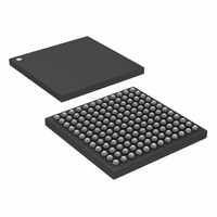
DS3154+ Maxim Integrated Products, DS3154+ Datasheet - Page 14

DS3154+
Manufacturer Part Number
DS3154+
Description
IC LIU DS3/E3/STS1 QUAD 144CSBGA
Manufacturer
Maxim Integrated Products
Type
Line Interface Units (LIUs)r
Datasheet
1.DS3151.pdf
(61 pages)
Specifications of DS3154+
Number Of Drivers/receivers
4/4
Protocol
IEEE 1149.1
Voltage - Supply
3.135 V ~ 3.465 V
Mounting Type
Surface Mount
Package / Case
144-CSBGA
Lead Free Status / RoHS Status
Lead free / RoHS Compliant
Table 4-E. JTAG and Test Pin Descriptions
Note 1: Pin type I = input pin. Pin type O = output pin. Pin type P = power-supply pin.
Note 2: Pin type O3 is an output that can be tri-stated.
Note 3: Pin type I
Note 4: For pin names of the form PINn, n = LIU# = 1, 2, 3, or 4. PIN1 is on LIU 1, PIN2 is on LIU 2, etc.
Note 5: Section
Table 4-F. Transmitter Data Select Options
Note 1: This coding of the TDSA, TDSB, E3M, and STS bits allows AIS generation to be enabled by holding TDSA = 0 and changing TDSB
Note 2: If E3M and/or STS are changed when {TDSA,TDSB} ≠ 00, TDSA and TDSB must both be cleared to 0. After they are cleared, TDSA
Table 4-G. Receiver PRBS Pattern Select Options
TDSA
E3M
JTCLK
NAME
RD/DS
NAME
JTRST
D[7:0]
A[5:0]
JTDO
JTMS
TEST
JTDI
0
0
0
0
0
1
1
1
1
1
0
1
V
INT
V
DD
SS
from 0 to 1. The type of DS3 AIS signal is selected by the STS bit with E3M = 0.
and TDSB can be configured to transmit a pattern in the new operating mode.
14
TDSB
PU
STS
shows hardware mode and CPU bus mode pin assignments.
is an input with an internal 10kΩ pullup.
0
1
1
1
1
0
1
1
1
I/O
I/O
I/O
I
I
I
I
0
X
1
O
P
P
O
PU
PU
PU
PU
I
I
I
transaction, with R/W = 1 indicating a read and R/W = 0 indicating a write.
Read Enable (Active Low) or Data Strobe (Active Low). In Intel bus mode (MOT = 0), RD is asserted
to read internal registers. In Motorola bus mode (MOT = 1), the rising edge of DS writes data to
internal registers.
Address Bus. These inputs specify the address of the internal register to be accessed. A5 is not
present on the DS3152. A5 and A4 are not present on the DS3151.
Data Bus. These bidirectional lines are inputs during writes to internal registers. They are outputs
during reads from internal registers.
Interrupt Output (Active Low, Open Drain). This pin is forced low in response to one or more
unmasked, active interrupt sources within the device. INT remains low until the interrupt is serviced or
masked.
Positive Supply. 3.3V ±5%. All V
Ground Reference. All V
JTAG IEEE 1149.1 Test Serial Clock. JTCLK shifts data into JTDI on the rising edge and out of
JTDO on the falling edge. If boundary scan is not used, JTCLK should be pulled high.
JTAG IEEE 1149.1 Test Serial-Data Input (Internal 10kΩ Pullup). Test instructions and data are
clocked in on this pin on the rising edge of JTCLK. If boundary scan is not used, JTDI should be left
unconnected or pulled high.
JTAG IEEE 1149.1 Test Serial-Data Output. Test instructions and data are clocked out on this pin on
the falling edge of JTCLK.
JTAG IEEE 1149.1 Test Reset (Internal 10kΩ Pullup). This pin is used to asynchronously reset the
test access port (TAP) controller. If boundary scan is not used, JTRST can be held low or high.
JTAG IEEE 1149.1 Test Mode Select (Internal 10kΩ Pullup). This pin is sampled on the rising edge
of JTCLK and is used to place the port into the various defined IEEE 1149.1 states. If boundary scan
is not used, JTMS should be left unconnected or pulled high.
Factory Test Pin. Leave unconnected or wire high for normal operation.
E3M
Rx MODE
X
X
0
1
1
0
1
0
1
STS-1
DS3
E3
DS3151/DS3152/DS3153/DS3154 Single/Dual/Triple/Quad DS3/E3/STS-1 LIUs
STS
X
X
X
0
0
1
1
0
1
SS
signals should be wired together.
RECEIVER PRBS PATTERN SELECTED
Tx MODE
2
2
STS-1
STS-1
DD
23
15
DS3
DS3
DS3
Any
Any
E3
E3
14 of 61
- 1 PRBS pattern per ITU O.151
- 1 PRBS pattern per ITU O.151
signals should be wired together.
FUNCTION
FUNCTION
Normal data as input at TPOS and TNEG
DS3 AIS per ANSI T1.107
2
2
23
15
TRANSMIT DATA SELECTED
- 1 PRBS pattern per ITU O.151
- 1 PRBS pattern per ITU O.151
Unframed 100100… pattern
Unframed all ones
(Figure
7-2)


