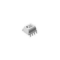
FDS6676S Fairchild Semiconductor, FDS6676S Datasheet - Page 2

FDS6676S
Manufacturer Part Number
FDS6676S
Description
MOSFET Power 30V N-Ch PowerTrench
Manufacturer
Fairchild Semiconductor
Datasheet
1.FDS6676S.pdf
(6 pages)
Specifications of FDS6676S
Configuration
Single Quad Drain Triple Source
Transistor Polarity
N-Channel
Resistance Drain-source Rds (on)
0.0052 Ohms
Drain-source Breakdown Voltage
30 V
Gate-source Breakdown Voltage
+/- 16 V
Continuous Drain Current
14.5 A
Power Dissipation
2.5 W
Maximum Operating Temperature
+ 150 C
Mounting Style
SMD/SMT
Package / Case
SOIC-8 Narrow
Minimum Operating Temperature
- 55 C
Lead Free Status / Rohs Status
In Transition
Other names
FDS6676S_NL
Available stocks
Company
Part Number
Manufacturer
Quantity
Price
Part Number:
FDS6676S
Manufacturer:
FAIRCHILD/仙童
Quantity:
20 000
Notes:
1. R
Scale 1 : 1 on letter size paper
Pulse Test: Pulse Width < 300 s, Duty Cycle < 2.0%
Electrical Characteristics
Symbol
Off Characteristics
BV
I
I
I
On Characteristics
V
R
I
g
Dynamic Characteristics
C
C
C
Switching Characteristics
t
t
t
t
Q
Q
Q
Drain–Source Diode Characteristics and Maximum Ratings
V
t
I
Q
R
the drain pins. R
DSS
GSSF
GSSR
D(on)
d(on)
r
d(off)
f
rr
RM
FS
BV
V
GS(th)
SD
DS(on)
iss
oss
rss
g
gs
gd
rr
G
JA
GS(th)
DSS
T
T
is the sum of the junction-to-case and case-to-ambient thermal resistance where the case thermal reference is defined as the solder mounting surface of
DSS
J
J
Drain–Source Breakdown Voltage
Breakdown Voltage Temperature
Coefficient
Zero Gate Voltage Drain Current
Gate–Body Leakage, Forward
Gate–Body Leakage, Reverse
Gate Threshold Voltage
Gate Threshold Voltage
Temperature Coefficient
Static Drain–Source
On–Resistance
On–State Drain Current
Forward Transconductance
Input Capacitance
Output Capacitance
Reverse Transfer Capacitance
Gate Resistance
Turn–On Delay Time
Turn–On Rise Time
Turn–Off Delay Time
Turn–Off Fall Time
Total Gate Charge
Gate–Source Charge
Gate–Drain Charge
Drain–Source Diode Forward
Voltage
Diode Reverse Recovery Time
Diode Reverse Recovery Current
Diode Reverse Recovery Charge
JC
is guaranteed by design while R
a) 50°/W when
mounted on a 1 in
pad of 2 oz copper
Parameter
(Note 2)
2
(Note 2)
CA
is determined by the user's board design.
T
V
I
V
V
V
V
I
V
V
V
V
V
V
f = 1.0 MHz
V
V
V
V
V
V
V
I
d
A
b) 105°/W when
D
D
F
= 25°C unless otherwise noted
iF
GS
DS
GS
GS
DS
GS
GS
GS
GS
DS
DS
GS
DD
GS
DS
GS
GS
GS
= 14.5A,
= 1 mA, Referenced to 25 C
= 1 mA, Referenced to 25 C
/d
mounted on a .04 in
pad of 2 oz copper
=10 V, I
= 24 V,
= V
= 10 V,
= 15 V,
= 15 V,
= 0 V,
= 16 V,
= –16 V,
= 10 V,
= 4.5 V,
= 10 V,
= 15 mV,
= 15 V,
= 10 V,
= 5 V
= 0 V,
= 0 V,
t
= 300 A/µs
Test Conditions
GS
,
D
I
I
=14.5A, T
S
S
= 3.5 A
= 7 A
I
V
V
V
I
I
I
V
I
I
R
D
D
D
D
D
D
V
GS
DS
DS
DS
GEN
f = 1.0 MHz
I
= 1 mA
= 1 mA
= 14.5 A
= 13.2 A
= 14.5 A
= 1 A,
D
2
GS
= 0 V
= 0 V
= 5 V
= 0 V
= 14.5 A,
= 6
= 0 V,
J
=125 C
(Note 2)
(Note 2)
(Note 3)
Min Typ
30
50
1
c) 125°/W when mounted on a
See “SyncFET Schottky body diode
characteristics” below
minimum pad.
4665
–3.8
5.25
826
304
390
490
1.4
6.0
8.0
1.4
1.8
21
80
11
10
82
30
43
10
11
31
30
Max
–100
500
100
131
700
7.5
9.0
12
20
20
48
60
3
FDS6676S Rev F1 (W)
Units
mV/ C
mV/ C
m
mV
nA
nA
pF
pF
pF
nC
nC
nC
nS
nC
ns
ns
ns
ns
V
V
A
S
A
A


