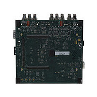
ADDS-BF533-EZLITE Analog Devices Inc, ADDS-BF533-EZLITE Datasheet - Page 10

ADDS-BF533-EZLITE
Manufacturer Part Number
ADDS-BF533-EZLITE
Description
Manufacturer
Analog Devices Inc
Datasheet
1.ADDS-BF533-EZLITE.pdf
(60 pages)
Specifications of ADDS-BF533-EZLITE
Significant Other Parts
ADV7183 Video Decode
Lead Free Status / Rohs Status
Not Compliant
ADSP-BF531/ADSP-BF532/ADSP-BF533
An additional 250 mV of SPORT input hysteresis can be
enabled by setting Bit 15 of the PLL_CTL register. When this bit
is set, all SPORT input pins have the increased hysteresis.
SERIAL PERIPHERAL INTERFACE (SPI) PORT
The ADSP-BF531/ADSP-BF532/ADSP-BF533 processor has an
SPI-compatible port that enables the processor to communicate
with multiple SPI-compatible devices.
The SPI interface uses three pins for transferring data: two data
pins (master output-slave input, MOSI, and master input-slave
output, MISO) and a clock pin (serial clock, SCK). An SPI chip
select input pin (SPISS) lets other SPI devices select the proces
sor, and seven SPI chip select output pins (SPISEL7–1) let the
processor select other SPI devices. The SPI select pins are recon-
figured general-purpose I/O pins. Using these pins, the SPI port
provides a full-duplex, synchronous serial interface which sup
ports both master/slave modes and multimaster environments.
The baud rate and clock phase/polarities for the SPI port are
programmable, and it has an integrated DMA controller, con
figurable to support transmit or receive data streams. The SPI
DMA controller can only service unidirectional accesses at any
given time.
The SPI port clock rate is calculated as:
Where the 16-bit SPI_BAUD register contains a value of 2 to
65,535.
During transfers, the SPI port simultaneously transmits and
receives by serially shifting data in and out on its two serial data
lines. The serial clock line synchronizes the shifting and sam
pling of data on the two serial data lines.
UART PORT
The ADSP-BF531/ADSP-BF532/ADSP-BF533 processor pro
vides a full-duplex universal asynchronous receiver/transmitter
(UART) port, which is fully compatible with PC-standard
UARTs. The UART port provides a simplified UART interface
to other peripherals or hosts, supporting full-duplex, DMA-sup
ported, asynchronous transfers of serial data. The UART port
includes support for 5 data bits to 8 data bits, 1 stop bit or 2 stop
bits, and none, even, or odd parity. The UART port supports
two modes of operation:
• Interrupts – Each transmit and receive port generates an
• Multichannel capability – Each SPORT supports 128 chan
• PIO (programmed I/O) – The processor sends or receives
• DMA (direct memory access) – The DMA controller trans
interrupt upon completing the transfer of a data-word or
after transferring an entire data buffer or buffers
through DMA.
nels out of a 1,024-channel window and is compatible with
the H.100, H.110, MVIP-90, and HMVIP standards.
data by writing or reading I/O-mapped UART registers.
The data is double-buffered on both transmit and receive.
fers both transmit and receive data. This reduces the
number and frequency of interrupts required to transfer
SPI Clock Rate = ----------------------------------- -
2 × SPI_BAUD
f
SCLK
Rev. E | Page 10 of 60 | July 2007
The baud rate, serial data format, error code generation and sta
tus, and interrupts for the UART port are programmable.
The UART programmable features include:
The UART port’s clock rate is calculated as:
Where the 16-bit UART_Divisor comes from the UART_DLH
register (most significant 8 bits) and UART_DLL register (least
significant 8 bits).
In conjunction with the general-purpose timer functions,
autobaud detection is supported.
The capabilities of the UART are further extended with support
for the Infrared Data Association (IrDA) serial infrared physical
layer link specification (SIR) protocol.
GENERAL-PURPOSE I/O PORT F
The ADSP-BF531/ADSP-BF532/ADSP-BF533 processor has 16
bidirectional, general-purpose I/O pins on Port F (PF15–0).
Each general-purpose I/O pin can be individually controlled by
manipulation of the GPIO control, status and interrupt
registers:
• Supporting bit rates ranging from (f
• Supporting data formats from seven bits to 12 bits per
• Both transmit and receive operations can be configured to
• GPIO direction control register – Specifies the direction of
• GPIO control and status registers – The ADSP-BF531/
• GPIO interrupt mask registers – The two GPIO interrupt
data to and from memory. The UART has two dedicated
DMA channels, one for transmit and one for receive. These
DMA channels have lower default priority than most DMA
channels because of their relatively low service rates.
second to (f
frame.
generate maskable interrupts to the processor.
each individual PFx pin as input or output.
ADSP-BF532/ADSP-BF533 processor employs a “write one
to modify” mechanism that allows any combination of
individual GPIO pins to be modified in a single instruction,
without affecting the level of any other GPIO pins. Four
control registers are provided. One register is written in
order to set GPIO pin values, one register is written in
order to clear GPIO pin values, one register is written in
order to toggle GPIO pin values, and one register is written
in order to specify GPIO pin values. Reading the GPIO sta
tus register allows software to interrogate the sense of the
GPIO pin.
mask registers allow each individual PFx pin to function as
an interrupt to the processor. Similar to the two GPIO con
trol registers that are used to set and clear individual GPIO
pin values, one GPIO interrupt mask register sets bits to
enable interrupt function, and the other GPIO interrupt
mask register clears bits to disable interrupt function. PFx
UART Clock Rate = ---------------------------------------------- -
SCLK
/16) bits per second.
16 × UART_Divisor
f
SCLK
SCLK
/1,048,576) bits per


