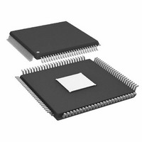
AD9957BSVZ Analog Devices Inc, AD9957BSVZ Datasheet - Page 47

AD9957BSVZ
Manufacturer Part Number
AD9957BSVZ
Description
IC DDS 1GSPS 14BIT IQ 100TQFP
Manufacturer
Analog Devices Inc
Datasheet
1.AD9957BSVZ-REEL.pdf
(64 pages)
Specifications of AD9957BSVZ
Resolution (bits)
14 b
Master Fclk
1GHz
Tuning Word Width (bits)
32 b
Voltage - Supply
1.8V, 3.3V
Operating Temperature
-40°C ~ 85°C
Mounting Type
Surface Mount
Package / Case
100-TQFP Exposed Pad, 100-eTQFP, 100-HTQFP, 100-VQFP
Frequency Range
60MHz To 1GHz
Rf Type
Quadrature
Supply Voltage Range
1.71V To 1.89V, 3.135V To 3.465
Rf Ic Case Style
TQFP
No. Of Pins
100
Operating Temperature Range
-40°C To +85°C
Operating Temperature (max)
85C
Operating Temperature (min)
-40C
Pin Count
100
Mounting
Surface Mount
Case Height
1mm
Screening Level
Industrial
Lead Free Status / RoHS Status
Lead free / RoHS Compliant
For Use With
AD9957/PCBZ - BOARD EVAL AD9957 QUADRATURE MOD
Lead Free Status / Rohs Status
Compliant
Available stocks
Company
Part Number
Manufacturer
Quantity
Price
Company:
Part Number:
AD9957BSVZ
Manufacturer:
AD
Quantity:
1 200
Company:
Part Number:
AD9957BSVZ
Manufacturer:
Analog Devices Inc
Quantity:
10 000
Part Number:
AD9957BSVZ
Manufacturer:
ADI/亚德诺
Quantity:
20 000
Company:
Part Number:
AD9957BSVZ-REEL
Manufacturer:
Analog Devices Inc
Quantity:
10 000
Part Number:
AD9957BSVZ-REEL
Manufacturer:
ADI/亚德诺
Quantity:
20 000
SERIAL PROGRAMMING
CONTROL INTERFACE—SERIAL I/O
The AD9957 serial port is a flexible, synchronous serial commu-
nications port allowing easy interface to many industry-standard
microcontrollers and microprocessors.
The interface allows read/write access to all registers that configure
the AD9957. MSB-first or LSB-first transfer formats are sup-
ported. In addition, the serial interface port can be configured
as a single pin input/output (SDIO) allowing a two-wire interface,
or it can be configured as two unidirectional pins for input/output
(SDIO/SDO), enabling a 3-wire interface. Two optional pins
(I/O_RESET and CS ) enable greater flexibility for designing
systems with the AD9957.
GENERAL SERIAL I/O OPERATION
There are two phases to a serial communications cycle. The first
is the instruction phase to write the instruction byte into the
AD9957. The instruction byte contains the address of the regis-
ter to be accessed (see the Register Map and Bit Descriptions
section) and defines whether the upcoming data transfer is a
write or read operation.
For a write cycle, Phase 2 represents the data transfer between
the serial port controller to the serial port buffer. The number
of bytes transferred is a function of the register being accessed.
For example, when accessing the Control Function Register 2
(Address 0x01), Phase 2 requires that four bytes be transferred.
Each bit of data is registered on each corresponding rising edge
of SCLK. The serial port controller expects that all bytes of the
register be accessed; otherwise, the serial port controller is put
out of sequence for the next communication cycle. However,
one way to write fewer bytes than required is to use the I/O_RESET
pin feature. The I/O_RESET pin function can be used to abort
an I/O operation and reset the pointer of the serial port con-
troller. After an I/O reset, the next byte is the instruction byte.
Note that every completed byte written prior to an I/O reset is
preserved in the serial port buffer. Partial bytes written are not
preserved. At the completion of any communication cycle, the
AD9957 serial port controller expects the next eight rising
SCLK edges to be the instruction byte for the next communi-
cation cycle.
After a write cycle, the programmed data resides in the serial
port buffer and is inactive. I/O_UPDATE transfers data from
the serial port buffer to active registers. The I/O update can
either be sent after each communication cycle or when all serial
operations are complete. In addition, a change in profile pins
can initiate an I/O update.
Rev. B | Page 47 of 64
For a read cycle, Phase 2 is the same as the write cycle with the
following differences: Data is read from the active registers, not
the serial port buffer, and data is driven out on the falling edge
of SCLK.
Note that to read back any profile register (0x0E to 0x15), the
three external profile pins must be used. For example, if the
profile register is Profile 5 (0x13) then PROFILE<0:2> pins
must equal 101.This is not required to write to profile registers.
INSTRUCTION BYTE
The instruction byte contains the following information as
shown in the instruction byte bit map.
Instruction Byte Information Bit Map
MSB
D7
R/W
R/ W —Bit 7 of the instruction byte determines whether a read
or write data transfer occurs after the instruction byte write.
Logic 1 indicates a read operation. Cleared indicates a write
operation.
X, X—Bit 6 and Bit 5 of the instruction byte are don’t cares.
A4, A3, A2, A1, A0—Bit 4, Bit 3, Bit 2, Bit 1, and Bit 0 of the
instruction byte determine which register is accessed during the
data transfer portion of the communications cycle.
SERIAL I/O PORT PIN DESCRIPTIONS
SCLK—Serial Clock
The serial clock pin is used to synchronize data to and from the
AD9957 and to run the internal state machines.
CS —Chip Select Bar
An active low input that allows more than one device on the
same serial communications line. The SDO and SDIO pins go
to a high impedance state when this input is high. If driven high
during any communications cycle, that cycle is suspended until
CS is reactivated low. Chip select ( CS ) can be tied low in
systems that maintain control of SCLK.
SDIO—Serial Data Input/Output
Data is always written into the AD9957 on this pin. However,
this pin can be used as a bidirectional data line. Bit 1 of CFR1,
Register Address 0x00, controls the configuration of this pin.
The default is cleared, which configures the SDIO pin as
bidirectional.
D6
X
D5
X
D4
A4
D3
A3
D2
A2
D1
A1
AD9957
LSB
D0
A0


