AD9957BSVZ Analog Devices Inc, AD9957BSVZ Datasheet - Page 18
AD9957BSVZ
Manufacturer Part Number
AD9957BSVZ
Description
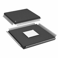
IC DDS 1GSPS 14BIT IQ 100TQFP
Manufacturer
Analog Devices Inc
Datasheet
1.AD9957BSVZ-REEL.pdf
(64 pages)
Specifications of AD9957BSVZ
Resolution (bits)
14 b
Master Fclk
1GHz
Tuning Word Width (bits)
32 b
Voltage - Supply
1.8V, 3.3V
Operating Temperature
-40°C ~ 85°C
Mounting Type
Surface Mount
Package / Case
100-TQFP Exposed Pad, 100-eTQFP, 100-HTQFP, 100-VQFP
Frequency Range
60MHz To 1GHz
Rf Type
Quadrature
Supply Voltage Range
1.71V To 1.89V, 3.135V To 3.465
Rf Ic Case Style
TQFP
No. Of Pins
100
Operating Temperature Range
-40°C To +85°C
Operating Temperature (max)
85C
Operating Temperature (min)
-40C
Pin Count
100
Mounting
Surface Mount
Case Height
1mm
Screening Level
Industrial
Lead Free Status / RoHS Status
Lead free / RoHS Compliant
For Use With
AD9957/PCBZ - BOARD EVAL AD9957 QUADRATURE MOD
Lead Free Status / Rohs Status
Compliant
Available stocks
Company
Part Number
Manufacturer
Quantity
Price
Company:

Part Number:
AD9957BSVZ
Manufacturer:
AD
Quantity:
1 200
Company:
Part Number:
AD9957BSVZ
Manufacturer:
Analog Devices Inc
Quantity:
10 000
Part Number:
AD9957BSVZ
Manufacturer:
ADI/亚德诺
Quantity:
20 000
Company:
Part Number:
AD9957BSVZ-REEL
Manufacturer:
Analog Devices Inc
Quantity:
10 000
Part Number:
AD9957BSVZ-REEL
Manufacturer:
ADI/亚德诺
Quantity:
20 000


AD9957
BLACKFIN INTERFACE (BFI) MODE
A subset of the QDUC mode is the Blackfin interface (BFI)
mode, shown in Figure 27; grayed items are inactive. In this
mode, a separate I and Q serial bit stream is applied to the
baseband data port instead of parallel data-words. The two
serial inputs provide for 16-bit I- and Q-words (unlike the
18-bit words in normal QDUC mode). The serial bit streams
are delivered to the Blackfin interface. The Blackfin interface
converts the 16-bit serial data into 16-bit parallel data to
propagate down the signal processing chain.
TxENABLE
PDCLK
I/Q IN
FTW
PW
2
TIMING AND CONTROL
PROGRAMMING
PARALLEL DATA
REGISTERS
3
18
16
16
18
QS
Q
IS
I
SERIAL I/O
PORT
Figure 27. Quadrature Modulation Mode, Blackfin Interface
INTERNAL CLOCK TIMING AND CONTROL
I Q
RAM
Rev. B | Page 18 of 64
IS QS
OSK
AD9957
cos (ωt+θ)
θ
ω
sin (ωt+θ)
CLOCK
CONTROL
DDS
POWER
DOWN
The Blackfin interface includes an additional pair of half-band
filters in both I and Q signal paths (not shown explicitly in the
diagram). The two half-band filters increase the interpolation
of the baseband data by a factor of four, relative to the normal
QDUC mode.
The synchronization of the serial data occurs through the
PDCLK signal. In BFI mode, the PDCLK signal is effectively
the bit clock for the serial data.
Note that the system clock is limited to 750 MHz in BFI mode.
2
2
SYSCLK
DAC GAIN
PLL
÷2
8
OUTPUT
FACTOR
SCALE
8-BIT
AUX
DAC
14-BIT
DAC
DAC_RSET
IOUT
IOUT
REFCLK_OUT
REF_CLK
REF_CLK
XTAL_SEL
Related parts for AD9957BSVZ
Image
Part Number
Description
Manufacturer
Datasheet
Request
R

Part Number:
Description:
D/A Converter Evaluation Board
Manufacturer:
Analog Devices Inc
Datasheet:


Part Number:
Description:
±1.7g Dual-Axis IMEMS Accelerometer Evaluation Board
Manufacturer:
Analog Devices Inc
Datasheet:

Part Number:
Description:
Inertial Sensor Evaluation System
Manufacturer:
Analog Devices Inc
Datasheet:
Part Number:
Description:
Manufacturer:
Analog Devices Inc
Datasheet:
Part Number:
Description:
Manufacturer:
Analog Devices Inc
Datasheet:
Part Number:
Description:
Manufacturer:
Analog Devices Inc
Datasheet:
Part Number:
Description:
Manufacturer:
Analog Devices Inc
Datasheet:
Part Number:
Description:
Manufacturer:
Analog Devices Inc
Datasheet:
Part Number:
Description:
Manufacturer:
Analog Devices Inc
Datasheet:
Part Number:
Description:
Manufacturer:
Analog Devices Inc
Datasheet:
Part Number:
Description:
Manufacturer:
Analog Devices Inc
Datasheet:
Part Number:
Description:
Manufacturer:
Analog Devices Inc
Datasheet: