AD9957BSVZ Analog Devices Inc, AD9957BSVZ Datasheet - Page 2
AD9957BSVZ
Manufacturer Part Number
AD9957BSVZ
Description
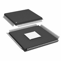
IC DDS 1GSPS 14BIT IQ 100TQFP
Manufacturer
Analog Devices Inc
Datasheet
1.AD9957BSVZ-REEL.pdf
(64 pages)
Specifications of AD9957BSVZ
Resolution (bits)
14 b
Master Fclk
1GHz
Tuning Word Width (bits)
32 b
Voltage - Supply
1.8V, 3.3V
Operating Temperature
-40°C ~ 85°C
Mounting Type
Surface Mount
Package / Case
100-TQFP Exposed Pad, 100-eTQFP, 100-HTQFP, 100-VQFP
Frequency Range
60MHz To 1GHz
Rf Type
Quadrature
Supply Voltage Range
1.71V To 1.89V, 3.135V To 3.465
Rf Ic Case Style
TQFP
No. Of Pins
100
Operating Temperature Range
-40°C To +85°C
Operating Temperature (max)
85C
Operating Temperature (min)
-40C
Pin Count
100
Mounting
Surface Mount
Case Height
1mm
Screening Level
Industrial
Lead Free Status / RoHS Status
Lead free / RoHS Compliant
For Use With
AD9957/PCBZ - BOARD EVAL AD9957 QUADRATURE MOD
Lead Free Status / Rohs Status
Compliant
Available stocks
Company
Part Number
Manufacturer
Quantity
Price
Company:

Part Number:
AD9957BSVZ
Manufacturer:
AD
Quantity:
1 200
Company:
Part Number:
AD9957BSVZ
Manufacturer:
Analog Devices Inc
Quantity:
10 000
Part Number:
AD9957BSVZ
Manufacturer:
ADI/亚德诺
Quantity:
20 000
Company:
Part Number:
AD9957BSVZ-REEL
Manufacturer:
Analog Devices Inc
Quantity:
10 000
Part Number:
AD9957BSVZ-REEL
Manufacturer:
ADI/亚德诺
Quantity:
20 000


AD9957
TABLE OF CONTENTS
Features .............................................................................................. 1
Applications ....................................................................................... 1
General Description ......................................................................... 1
Functional Block Diagram .............................................................. 1
Revision History ............................................................................... 4
Specifications ..................................................................................... 5
Absolute Maximum Ratings ............................................................ 8
Pin Configuration and Function Descriptions ............................. 9
Typical Performance Characteristics ........................................... 12
Modes of Operation ....................................................................... 16
Signal Processing ............................................................................ 21
Electrical Specifications ............................................................... 5
ESD Caution .................................................................................. 8
Overview ...................................................................................... 16
Quadrature Modulation Mode ................................................. 17
BlackFin Interface (BFI) Mode ................................................. 18
Interpolating DAC Mode .......................................................... 19
Single Tone Mode ....................................................................... 20
Parallel Data Clock (PDCLK) ................................................... 21
Transmit Enable Pin (TxEnable) .............................................. 21
Input Data Assembler ................................................................ 22
Inverse CCI Filter ....................................................................... 23
Fixed Interpolator (4×) .............................................................. 23
Programmable Interpolating Filter .......................................... 24
Quadrature Modulator .............................................................. 25
DDS Core ..................................................................................... 25
Inverse Sinc Filter ....................................................................... 25
Output Scale Factor (OSF) ........................................................ 26
14-Bit DAC .................................................................................. 26
QDUC Mode ........................................................................... 24
BFI Mode ................................................................................. 24
Auxiliary DAC ........................................................................ 26
Rev. B | Page 2 of 64
RAM Control .................................................................................. 27
Clock Input (REF_CLK) ................................................................ 34
Additional Features ........................................................................ 37
Synchronization of Multiple Devices ........................................... 40
RAM Overview ........................................................................... 27
RAM Segment Registers ............................................................ 27
RAM State Machine ................................................................... 27
RAM Trigger (RT) Pin ............................................................... 27
Load/Retrieve RAM Operation ................................................ 28
RAM Playback Operation ......................................................... 28
Overview of RAM Playback Modes ......................................... 29
REFCLK Overview ..................................................................... 34
Crystal Driven REF_CLK ......................................................... 34
Direct Driven REF_CLK ........................................................... 34
Phase-Locked Loop (PLL) Multiplier ...................................... 35
PLL Charge Pump ...................................................................... 36
External PLL Loop Filter Components ................................... 36
PLL Lock Indication .................................................................. 36
Output Shift Keying (OSK) ....................................................... 37
Profiles ......................................................................................... 38
I/O_UPDATE Pin ...................................................................... 38
Automatic I/O Update ............................................................... 38
Power-Down Control ................................................................ 39
General-Purpose I/O (GPIO) Port .......................................... 39
Overview ..................................................................................... 40
Clock Generator ......................................................................... 40
RAM Ramp-Up Mode ........................................................... 29
RAM Bidirectional Ramp Mode .......................................... 30
RAM Continuous Bidirectional Ramp Mode .................... 32
RAM Continuous Recirculate Mode ................................... 33
Manual OSK ............................................................................ 37
Automatic OSK ....................................................................... 37
Related parts for AD9957BSVZ
Image
Part Number
Description
Manufacturer
Datasheet
Request
R

Part Number:
Description:
D/A Converter Evaluation Board
Manufacturer:
Analog Devices Inc
Datasheet:


Part Number:
Description:
±1.7g Dual-Axis IMEMS Accelerometer Evaluation Board
Manufacturer:
Analog Devices Inc
Datasheet:

Part Number:
Description:
Inertial Sensor Evaluation System
Manufacturer:
Analog Devices Inc
Datasheet:
Part Number:
Description:
Manufacturer:
Analog Devices Inc
Datasheet:
Part Number:
Description:
Manufacturer:
Analog Devices Inc
Datasheet:
Part Number:
Description:
Manufacturer:
Analog Devices Inc
Datasheet:
Part Number:
Description:
Manufacturer:
Analog Devices Inc
Datasheet:
Part Number:
Description:
Manufacturer:
Analog Devices Inc
Datasheet:
Part Number:
Description:
Manufacturer:
Analog Devices Inc
Datasheet:
Part Number:
Description:
Manufacturer:
Analog Devices Inc
Datasheet:
Part Number:
Description:
Manufacturer:
Analog Devices Inc
Datasheet:
Part Number:
Description:
Manufacturer:
Analog Devices Inc
Datasheet: