AD9957BSVZ Analog Devices Inc, AD9957BSVZ Datasheet - Page 29
AD9957BSVZ
Manufacturer Part Number
AD9957BSVZ
Description
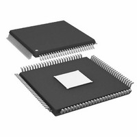
IC DDS 1GSPS 14BIT IQ 100TQFP
Manufacturer
Analog Devices Inc
Datasheet
1.AD9957BSVZ-REEL.pdf
(64 pages)
Specifications of AD9957BSVZ
Resolution (bits)
14 b
Master Fclk
1GHz
Tuning Word Width (bits)
32 b
Voltage - Supply
1.8V, 3.3V
Operating Temperature
-40°C ~ 85°C
Mounting Type
Surface Mount
Package / Case
100-TQFP Exposed Pad, 100-eTQFP, 100-HTQFP, 100-VQFP
Frequency Range
60MHz To 1GHz
Rf Type
Quadrature
Supply Voltage Range
1.71V To 1.89V, 3.135V To 3.465
Rf Ic Case Style
TQFP
No. Of Pins
100
Operating Temperature Range
-40°C To +85°C
Operating Temperature (max)
85C
Operating Temperature (min)
-40C
Pin Count
100
Mounting
Surface Mount
Case Height
1mm
Screening Level
Industrial
Lead Free Status / RoHS Status
Lead free / RoHS Compliant
For Use With
AD9957/PCBZ - BOARD EVAL AD9957 QUADRATURE MOD
Lead Free Status / Rohs Status
Compliant
Available stocks
Company
Part Number
Manufacturer
Quantity
Price
Company:

Part Number:
AD9957BSVZ
Manufacturer:
AD
Quantity:
1 200
Company:
Part Number:
AD9957BSVZ
Manufacturer:
Analog Devices Inc
Quantity:
10 000
Part Number:
AD9957BSVZ
Manufacturer:
ADI/亚德诺
Quantity:
20 000
Company:
Part Number:
AD9957BSVZ-REEL
Manufacturer:
Analog Devices Inc
Quantity:
10 000
Part Number:
AD9957BSVZ-REEL
Manufacturer:
ADI/亚德诺
Quantity:
20 000


OVERVIEW OF RAM PLAYBACK MODES
The RAM is operational in any one of four different
playback modes.
•
•
•
•
RAM playback is only functional when the AD9957 is pro-
grammed for either the QDUC or interpolating DAC mode.
The RAM playback mode is selected via the 3-bit RAM play-
back mode word located in each of the RAM segment registers.
Thus, the RAM playback mode is segment dependent. The
RAM playback mode bits are detailed in Table 5.
Table 5. RAM Playback Modes
RAM Playback Mode
Bits<2:0>
001
010
011
100
000, 101, 110, 111
The continuous bidirectional ramp and continuous recirculate
modes are not available when the baseband scaling multipliers
serve as the destination of RAM playback.
NOTES
1. NONESSENTIAL FUNCTIONAL COMPONENTS ARE RENDERED IN GRAY.
MACHINE
STATE
Ramp-up
Bidirectional ramp
Continuous bidirectional ramp
Continuous recirculate
CLK
16
10
UP/DOWN COUNTER
10
Figure 42. RAM Playback to Baseband Data Path
3
RAM MODE
ADDRESS STEP RATE
START ADDRESS
END ADDRESS
U/D
Q CHANNEL
Q
I CHANNEL
10
DDS CLOCK
BASEBAND DATA CLOCK
RAM
QS
IS
Q
I
(MSBs)
(LSBs)
32
16
16
RAM Playback Mode
Ramp-up
Bidirectional ramp
Continuous bidirectional
ramp
Continuous recirculate
Not Valid
32
REGISTERS
SEGMENT
RAM
RT
SDIO
SDO
SCLK
I/O_RESET
CS
Rev. B | Page 29 of 64
RAM Ramp-Up Mode
In ramp-up mode, upon assertion of an I/O update or a state
change on the RT pin, the RAM begins playback operation
using the parameters programmed into the selected RAM seg-
ment register. Data is extracted from RAM over the specified
address range contained in the start address and end address of
the active RAM segment register. The data is delivered at the
appropriate rate and to the destination as specified by the RAM
playback destination bit.
The playback rate is governed by the timer internal to the RAM
state machine and its period (Δt) is determined by the state of the
RAM playback destination bit as detailed in the RAM playback
operation section.
The internal state machine begins extracting data from the
RAM at the start address and continues to extract data until it
reaches the end address. Upon reaching this address, the state
machine halts.
A graphic representation of the ramp-up mode appears in
Figure 43. The upper trace shows the progression of the RAM
address from the start address to the end address for the active
RAM segment register. The address value advances by one with
each timeout of the timer internal to the state machine. The circled
numbers indicate specific events, explained as follows:
Event 1—an I/O update or state transition on the RT pin. This
event initializes the state machine to the start address of the active
RAM segment register.
Event 2—the state machine reaches the end address of the active
RAM segment register and halts.
I/O_UPDATE OR
RT TRANSITION
ADDRESS
RAM
M DDS CLOCK CYCLES
1 PDCLK CYCLE
Figure 43. Ramp-Up Timing Diagram
1
OR
END ADDRESS
START ADDRESS
1
Δ
t
2
AD9957
Related parts for AD9957BSVZ
Image
Part Number
Description
Manufacturer
Datasheet
Request
R

Part Number:
Description:
D/A Converter Evaluation Board
Manufacturer:
Analog Devices Inc
Datasheet:


Part Number:
Description:
±1.7g Dual-Axis IMEMS Accelerometer Evaluation Board
Manufacturer:
Analog Devices Inc
Datasheet:

Part Number:
Description:
Inertial Sensor Evaluation System
Manufacturer:
Analog Devices Inc
Datasheet:
Part Number:
Description:
Manufacturer:
Analog Devices Inc
Datasheet:
Part Number:
Description:
Manufacturer:
Analog Devices Inc
Datasheet:
Part Number:
Description:
Manufacturer:
Analog Devices Inc
Datasheet:
Part Number:
Description:
Manufacturer:
Analog Devices Inc
Datasheet:
Part Number:
Description:
Manufacturer:
Analog Devices Inc
Datasheet:
Part Number:
Description:
Manufacturer:
Analog Devices Inc
Datasheet:
Part Number:
Description:
Manufacturer:
Analog Devices Inc
Datasheet:
Part Number:
Description:
Manufacturer:
Analog Devices Inc
Datasheet:
Part Number:
Description:
Manufacturer:
Analog Devices Inc
Datasheet: