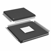
AD9957BSVZ Analog Devices Inc, AD9957BSVZ Datasheet - Page 45

AD9957BSVZ
Manufacturer Part Number
AD9957BSVZ
Description
IC DDS 1GSPS 14BIT IQ 100TQFP
Manufacturer
Analog Devices Inc
Datasheet
1.AD9957BSVZ-REEL.pdf
(64 pages)
Specifications of AD9957BSVZ
Resolution (bits)
14 b
Master Fclk
1GHz
Tuning Word Width (bits)
32 b
Voltage - Supply
1.8V, 3.3V
Operating Temperature
-40°C ~ 85°C
Mounting Type
Surface Mount
Package / Case
100-TQFP Exposed Pad, 100-eTQFP, 100-HTQFP, 100-VQFP
Frequency Range
60MHz To 1GHz
Rf Type
Quadrature
Supply Voltage Range
1.71V To 1.89V, 3.135V To 3.465
Rf Ic Case Style
TQFP
No. Of Pins
100
Operating Temperature Range
-40°C To +85°C
Operating Temperature (max)
85C
Operating Temperature (min)
-40C
Pin Count
100
Mounting
Surface Mount
Case Height
1mm
Screening Level
Industrial
Lead Free Status / RoHS Status
Lead free / RoHS Compliant
For Use With
AD9957/PCBZ - BOARD EVAL AD9957 QUADRATURE MOD
Lead Free Status / Rohs Status
Compliant
Available stocks
Company
Part Number
Manufacturer
Quantity
Price
Company:
Part Number:
AD9957BSVZ
Manufacturer:
AD
Quantity:
1 200
Company:
Part Number:
AD9957BSVZ
Manufacturer:
Analog Devices Inc
Quantity:
10 000
Part Number:
AD9957BSVZ
Manufacturer:
ADI/亚德诺
Quantity:
20 000
Company:
Part Number:
AD9957BSVZ-REEL
Manufacturer:
Analog Devices Inc
Quantity:
10 000
Part Number:
AD9957BSVZ-REEL
Manufacturer:
ADI/亚德诺
Quantity:
20 000
I/Q PATH LATENCY
The I/Q latency through the AD9957 is easiest to describe in
terms of system clock (SYSCLK) cycles and is a function of the
AD9957 configuration (that is, which mode and which optional
features are engaged). The I/Q latency is primarily affected by
the programmable CCI rate.
The values in Table 12 should be considered estimates because
observed latency may be data dependent. The latency was
calculated using the linear delay model for FIR filters. N = CCI
rate (programmable interpolation rate, 2 to 63, 1 if bypassed).
In BFI mode, the latency through the AD9957 may not be con-
stant for multiple transmissions. This is due to the relationship
between the phase of the clock that drives the first half-band
filter and the frame sync signal coming from the Blackfin,
which is unknown and denoted as x in Table 12. The design
successfully transfers data from the data assembler logic to the
Table 12.
Stage
Input Demuxplexer
Input Scale Multiplier
Inverse CCI Filter
Half-Band Filters
CCI Filter
Modulator
Inverse Sinc Filter
Output Scale Multiplier
DAC Interface
Quadrature Modulation Mode—Parallel
16N
Active: 8N
Bypassed: 4N
Active: 8N
Bypassed: 4N
69N
Active: 4N + 8
Bypass: 2N + 4
22
Active: 8
Bypass: 2
Active: 12
Bypass: 2
8
Rev. B | Page 45 of 64
Quadrature Modulation Mode—BFI
(16 + x)N
where x = 0 to 15
Not available in BFI mode
Active: 8N
Bypassed: 4N
345N
Active: 4N + 8
Bypass: 2N + 4
22
Active: 8
Bypass: 2
Active: 12
Bypass: 2
8
signal process path by updating a parallel register at the proper
time. The data is transferred from the parallel register to the
signal processing chain and all timing has been verified regard-
less of the phase relationship between the updating of the parallel
register and the signal processing clock.
Example
Quadrature modulation mode = 18-bit parallel data
Reference clock multiplier = bypassed
Input scale multiplier = off
Inverse CCI = off
CCI rate = 20
Inverse SINC = on
Output scale = off
Latency = (16 × 20) + (4 × 20) + (4 × 20) + (69 × 20) +
(4 × 20 + 8) + 22 + 8 + 2 + 8 = 1988 SYSCLKs
Interpolation DAC Mode
28N
Active: 8N
Bypassed: 4N
Active: 8N
Bypassed: 4N
69N
Active: 4N + 8
Bypass: 2N + 4
0
Active: 8
Bypass: 2
Active: 12
Bypass: 2
8
AD9957


