AD9957BSVZ Analog Devices Inc, AD9957BSVZ Datasheet - Page 43
AD9957BSVZ
Manufacturer Part Number
AD9957BSVZ
Description
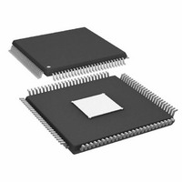
IC DDS 1GSPS 14BIT IQ 100TQFP
Manufacturer
Analog Devices Inc
Datasheet
1.AD9957BSVZ-REEL.pdf
(64 pages)
Specifications of AD9957BSVZ
Resolution (bits)
14 b
Master Fclk
1GHz
Tuning Word Width (bits)
32 b
Voltage - Supply
1.8V, 3.3V
Operating Temperature
-40°C ~ 85°C
Mounting Type
Surface Mount
Package / Case
100-TQFP Exposed Pad, 100-eTQFP, 100-HTQFP, 100-VQFP
Frequency Range
60MHz To 1GHz
Rf Type
Quadrature
Supply Voltage Range
1.71V To 1.89V, 3.135V To 3.465
Rf Ic Case Style
TQFP
No. Of Pins
100
Operating Temperature Range
-40°C To +85°C
Operating Temperature (max)
85C
Operating Temperature (min)
-40C
Pin Count
100
Mounting
Surface Mount
Case Height
1mm
Screening Level
Industrial
Lead Free Status / RoHS Status
Lead free / RoHS Compliant
For Use With
AD9957/PCBZ - BOARD EVAL AD9957 QUADRATURE MOD
Lead Free Status / Rohs Status
Compliant
Available stocks
Company
Part Number
Manufacturer
Quantity
Price
Company:

Part Number:
AD9957BSVZ
Manufacturer:
AD
Quantity:
1 200
Company:
Part Number:
AD9957BSVZ
Manufacturer:
Analog Devices Inc
Quantity:
10 000
Part Number:
AD9957BSVZ
Manufacturer:
ADI/亚德诺
Quantity:
20 000
Company:
Part Number:
AD9957BSVZ-REEL
Manufacturer:
Analog Devices Inc
Quantity:
10 000
Part Number:
AD9957BSVZ-REEL
Manufacturer:
ADI/亚德诺
Quantity:
20 000


The validation result latch is in a reset state whenever the sync
receiver is disabled, which forces the SYNC_SMP_ERR pin to a
Logic 0 state. To reset the validation result latch when the sync
receiver is active, however, requires the use of the Sync Timing
Validation Disable bit in the multichip sync register. To make a
setup/hold validation measurement is a two-step process. First,
write a Logic 1 to the sync timing validation disable bit. Then,
to make a measurement, write a Logic 0. The first action resets
the validation result latch and holds it in a reset state; the
second action releases the reset state and enables the validation
result latch to capture a setup/hold validation measurement.
Each time a new setup/hold validation check is desired, this
two-step procedure must be performed.
RECEIVER
SYSCLK
DELAY
LOGIC
FROM
SYNC
SYNC TIMING VALIDATION DISABLE
DELAY
DELAY
4
4
RISING EDGE
AND STROBE
SETUP AND HOLD VALIDATION
GENERATOR
Figure 58. Sync Timing Validation Block
DETECTOR
SYNC RECEIVER
4
D Q
SYNC VALIDATION
DELAY
Rev. B | Page 43 of 64
VALIDATION
D Q
VALIDATION
SETUP
PULSE
SYNC
HOLD
D Q
TO
CLOCK
GENERATION
LOGIC
Because the programmed value of the sync validation delay
establishes the time window for a setup/hold measurement,
the amount of delay is an important consideration for proper
operation of the validation block. The value chosen should
represent a small fraction of the SYSCLK period. For example,
if the SYSCLK frequency is 1 GHz (1000 ps period), then a
reasonable sync validation delay value is 2 (~300 ps). This
allows the validation block to ensure that the local SYSCLK
and the delayed SYNC_IN edges exhibit at least 300 ps of
timing separation. Choosing too large a value can cause the
validation block to indicate a setup/hold violation when one
does not exist. Choosing too small a value can cause the
validation block to miss a setup/hold violation when one
actually exists.
12
SYNC_SMP_ERR
AD9957
Related parts for AD9957BSVZ
Image
Part Number
Description
Manufacturer
Datasheet
Request
R

Part Number:
Description:
D/A Converter Evaluation Board
Manufacturer:
Analog Devices Inc
Datasheet:


Part Number:
Description:
±1.7g Dual-Axis IMEMS Accelerometer Evaluation Board
Manufacturer:
Analog Devices Inc
Datasheet:

Part Number:
Description:
Inertial Sensor Evaluation System
Manufacturer:
Analog Devices Inc
Datasheet:
Part Number:
Description:
Manufacturer:
Analog Devices Inc
Datasheet:
Part Number:
Description:
Manufacturer:
Analog Devices Inc
Datasheet:
Part Number:
Description:
Manufacturer:
Analog Devices Inc
Datasheet:
Part Number:
Description:
Manufacturer:
Analog Devices Inc
Datasheet:
Part Number:
Description:
Manufacturer:
Analog Devices Inc
Datasheet:
Part Number:
Description:
Manufacturer:
Analog Devices Inc
Datasheet:
Part Number:
Description:
Manufacturer:
Analog Devices Inc
Datasheet:
Part Number:
Description:
Manufacturer:
Analog Devices Inc
Datasheet:
Part Number:
Description:
Manufacturer:
Analog Devices Inc
Datasheet: