AD9957BSVZ Analog Devices Inc, AD9957BSVZ Datasheet - Page 35
AD9957BSVZ
Manufacturer Part Number
AD9957BSVZ
Description
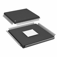
IC DDS 1GSPS 14BIT IQ 100TQFP
Manufacturer
Analog Devices Inc
Datasheet
1.AD9957BSVZ-REEL.pdf
(64 pages)
Specifications of AD9957BSVZ
Resolution (bits)
14 b
Master Fclk
1GHz
Tuning Word Width (bits)
32 b
Voltage - Supply
1.8V, 3.3V
Operating Temperature
-40°C ~ 85°C
Mounting Type
Surface Mount
Package / Case
100-TQFP Exposed Pad, 100-eTQFP, 100-HTQFP, 100-VQFP
Frequency Range
60MHz To 1GHz
Rf Type
Quadrature
Supply Voltage Range
1.71V To 1.89V, 3.135V To 3.465
Rf Ic Case Style
TQFP
No. Of Pins
100
Operating Temperature Range
-40°C To +85°C
Operating Temperature (max)
85C
Operating Temperature (min)
-40C
Pin Count
100
Mounting
Surface Mount
Case Height
1mm
Screening Level
Industrial
Lead Free Status / RoHS Status
Lead free / RoHS Compliant
For Use With
AD9957/PCBZ - BOARD EVAL AD9957 QUADRATURE MOD
Lead Free Status / Rohs Status
Compliant
Available stocks
Company
Part Number
Manufacturer
Quantity
Price
Company:

Part Number:
AD9957BSVZ
Manufacturer:
AD
Quantity:
1 200
Company:
Part Number:
AD9957BSVZ
Manufacturer:
Analog Devices Inc
Quantity:
10 000
Part Number:
AD9957BSVZ
Manufacturer:
ADI/亚德诺
Quantity:
20 000
Company:
Part Number:
AD9957BSVZ-REEL
Manufacturer:
Analog Devices Inc
Quantity:
10 000
Part Number:
AD9957BSVZ-REEL
Manufacturer:
ADI/亚德诺
Quantity:
20 000


PHASE-LOCKED LOOP (PLL) MULTIPLIER
An internal phase-locked loop (PLL) provides users of the
AD9957 the option to use a reference clock frequency that is
significantly lower than the system clock frequency. The PLL
supports a wide range of programmable frequency multiplica-
tion factors (12× to 127×) as well as a programmable charge
pump current and external loop filter components (connected
via the PLL_LOOP_FILTER pin). These features add an extra
layer of flexibility to the PLL, allowing optimization of phase
noise performance and flexibility in frequency plan develop-
ment. The PLL is also equipped with a PLL_LOCK pin.
The PLL output frequency range (f
range of 420 MHz ≤ f
addition, the user must program the VCO to one of six operating
ranges such that f
and Figure 51 summarize these VCO ranges.
Figure 50 shows the boundaries of the VCO frequency ranges
over the full range of temperature and supply voltage variation
for all devices from the available population. The implication is
that multiple devices chosen at random from the population and
operated under widely varying conditions may require different
values to be programmed into CFR3<26:24> to operate at the
same frequency. For example, Part A chosen randomly from the
population, operating in an ambient temperature of −10°C with
a system clock frequency of 900 MHz may require CFR3<26:24>
to be set to 100b. Whereas Part B chosen randomly from the
population, operating in an ambient temperature of 90°C with a
system clock frequency of 900 MHz may require CFR3<26:24>
to be set to 101b. If a frequency plan is chosen such that the
system clock frequency operates within one set of boundaries
(as shown in Figure 51), the required value in CFR3<26:24> is
consistent from part to part.
SINGLE-ENDED SOURCE,
SINGLE-ENDED SOURCE,
DIFFERENTIAL SOURCE,
SINGLE-ENDED INPUT.
DIFFERENTIAL INPUT.
DIFFERENTIAL INPUT.
Figure 49. Direct Connection Diagram
SYSCLK
SYSCLK
falls within the specified range. Figure 50
LVPECL,
DRIVER
PECL,
LVDS
≤ 1 GHz by the internal VCO. In
OR
BALUN
50Ω
(1:1)
SYSCLK
TERMINATION
) is constrained to the
50Ω
0.1µF
0.1µF
0.1µF
0.1µF
0.1µF
0.1µF
90
91
90
91
90
91
REF_CLK
REF_CLK
REF_CLK
REF_CLK
REF_CLK
REF_CLK
Rev. B | Page 35 of 64
Figure 51 shows the boundaries of the VCO frequency ranges
over the full range of temperature and supply voltage variation
for an individual device selected from the population. Figure 51
shows that the VCO frequency ranges for a single device always
overlap when operated over the full range of conditions.
In conclusion, if a user wants to retain a single default value for
CFR3<26:24>, a frequency that falls into one of the ranges
found in Figure 50 should be selected. Additionally, for any
given individual device, the VCO frequency ranges overlap,
meaning that any given device exhibits no gaps in its frequency
coverage across VCO ranges over the full range of conditions.
Table 7. VCO Range Bit Settings
VCO SEL Bits
(CFR3<26:24>)
000
001
010
011
100
101
110
111
VCO5
VCO4
VCO3
VCO2
VCO1
VCO0
VCO5
VCO4
VCO3
VCO2
VCO1
VCO0
Figure 50. VCO Ranges Including Atypical Wafer Process Skew
395
335
435
FLOW = 400
FHIGH = 460
495
FHIGH = 966
FLOW = 646
Figure 51. Typical VCO Ranges
535
FLOW = 455
FHIGH = 530
FLOW = 342
FHIGH = 522
595
FHIGH = 1180
635
FLOW = 402
FHIGH = 602
FLOW = 810
FHIGH = 875
VCO Range
VCO0
VCO1
VCO2
VCO3
VCO4
VCO5
PLL Bypassed
PLL Bypassed
FLOW = 760
FLOW = 530
FHIGH = 615
695
735
(MHz)
(MHz)
FLOW = 469
FHIGH = 709
835
FHIGH = 1030
795
FLOW = 920
FLOW = 650
FHIGH = 790
FLOW = 574
FHIGH = 904
935
895
1035
AD9957
1135
995
Related parts for AD9957BSVZ
Image
Part Number
Description
Manufacturer
Datasheet
Request
R

Part Number:
Description:
D/A Converter Evaluation Board
Manufacturer:
Analog Devices Inc
Datasheet:


Part Number:
Description:
±1.7g Dual-Axis IMEMS Accelerometer Evaluation Board
Manufacturer:
Analog Devices Inc
Datasheet:

Part Number:
Description:
Inertial Sensor Evaluation System
Manufacturer:
Analog Devices Inc
Datasheet:
Part Number:
Description:
Manufacturer:
Analog Devices Inc
Datasheet:
Part Number:
Description:
Manufacturer:
Analog Devices Inc
Datasheet:
Part Number:
Description:
Manufacturer:
Analog Devices Inc
Datasheet:
Part Number:
Description:
Manufacturer:
Analog Devices Inc
Datasheet:
Part Number:
Description:
Manufacturer:
Analog Devices Inc
Datasheet:
Part Number:
Description:
Manufacturer:
Analog Devices Inc
Datasheet:
Part Number:
Description:
Manufacturer:
Analog Devices Inc
Datasheet:
Part Number:
Description:
Manufacturer:
Analog Devices Inc
Datasheet:
Part Number:
Description:
Manufacturer:
Analog Devices Inc
Datasheet: