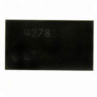
LTC4278CDKD#PBF Linear Technology, LTC4278CDKD#PBF Datasheet - Page 39

LTC4278CDKD#PBF
Manufacturer Part Number
LTC4278CDKD#PBF
Description
IC PD IEEE 802.3AT 25.5W 32-DFN
Manufacturer
Linear Technology
Datasheet
1.LTC4278CDKDPBF.pdf
(40 pages)
Specifications of LTC4278CDKD#PBF
Controller Type
Powered Device Interface Controller (PD)
Interface
IEEE 802.3af
Voltage - Supply
4.5 V ~ 20 V
Current - Supply
6.4mA
Operating Temperature
0°C ~ 70°C
Mounting Type
Surface Mount
Package / Case
32-DFN
Input Voltage
60V
Supply Current
1.35mA
Digital Ic Case Style
DFN
No. Of Pins
32
Duty Cycle (%)
88%
Frequency
100kHz
Operating Temperature Range
°C To +70°C
Msl
MSL 1 - Unlimited
Rohs Compliant
Yes
Lead Free Status / RoHS Status
Lead free / RoHS Compliant
Available stocks
Company
Part Number
Manufacturer
Quantity
Price
PACKAGE DESCRIPTION
4.50 ± 0.05
3.10 ± 0.05
0.200 REF
NOTE:
1. DRAWING PROPOSED TO BE MADE VARIATION OF VERSION (WXXX)
2. DRAWING NOT TO SCALE
3. ALL DIMENSIONS ARE IN MILLIMETERS
IN JEDEC PACKAGE OUTLINE M0-229
APPLY SOLDER MASK TO AREAS THAT ARE NOT SOLDERED
2.65 ±0.05
PIN 1
TOP MARK
(SEE NOTE 6)
RECOMMENDED SOLDER PAD LAYOUT
0.40 BSC
6.43 ±0.05
7.00 ±0.10
Information furnished by Linear Technology Corporation is believed to be accurate and reliable.
However, no responsibility is assumed for its use. Linear Technology Corporation makes no representa-
tion that the interconnection of its circuits as described herein will not infringe on existing patent rights.
6.00 REF
0.20 ± 0.05
(Reference LTC DWG # 05-08-1734 Rev A)
32-Lead Plastic DFN (7mm × 4mm)
0.00 – 0.05
0.75 ±0.05
DKD Package
0.70 ± 0.05
4.00 ±0.10
PACKAGE
OUTLINE
4. DIMENSIONS OF EXPOSED PAD ON BOTTOM OF PACKAGE DO NOT INCLUDE
5. EXPOSED PAD SHALL BE SOLDER PLATED
6. SHADED AREA IS ONLY A REFERENCE FOR PIN 1 LOCATION
MOLD FLASH. MOLD FLASH, IF PRESENT, SHALL NOT EXCEED 0.20mm ON ANY SIDE
ON THE TOP AND BOTTOM OF PACKAGE
R = 0.05
TYP
17
16
2.65 ±0.10
BOTTOM VIEW—EXPOSED PAD
6.43 ±0.10
0.40 BSC
R = 0.115
TYP
6.00 REF
0.35 × 45° CHAMFER
R = 0.30 TYP OR
PIN 1 NOTCH
0.20 ± 0.05
LTC4278
(DKD32) QFN 0707 REV A
32
1
39
0.40 ± 0.10
4278fa


