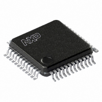
UCB1400BE,151 NXP Semiconductors, UCB1400BE,151 Datasheet - Page 7

UCB1400BE,151
Manufacturer Part Number
UCB1400BE,151
Description
IC AUDIO CODEC 3.3V 48-LQFP
Manufacturer
NXP Semiconductors
Type
Audio Codec '97r
Datasheet
1.UCB1400BEFE.pdf
(63 pages)
Specifications of UCB1400BE,151
Package / Case
48-LQFP
Data Interface
Serial
Resolution (bits)
20 b
Number Of Adcs / Dacs
2 / 2
Sigma Delta
No
S/n Ratio, Adcs / Dacs (db) Typ
97 / 91
Voltage - Supply, Analog
3 V ~ 3.6 V
Voltage - Supply, Digital
3 V ~ 3.6 V
Operating Temperature
-40°C ~ 85°C
Mounting Type
Surface Mount
Mounting Style
SMD/SMT
Lead Free Status / RoHS Status
Lead free / RoHS Compliant
Other names
935269304151
UCB1400BE-SNXP
UCB1400BE-SNXP
UCB1400BE-SNXP
UCB1400BE-SNXP
Available stocks
Company
Part Number
Manufacturer
Quantity
Price
Company:
Part Number:
UCB1400BE,151
Manufacturer:
NXP Semiconductors
Quantity:
10 000
Philips Semiconductors
9397 750 09611
Product data
Fig 5. Standard bi-directional audio frame.
SDATA_OUT
SDATA_IN
SLOT #
SYNC
CODEC ID
SLOTREQ 3–12
TAG
TAG
8.3.1 AC-link digital serial interface protocol
0
8.3 Digital interface
STATUS
ADDR
ADDR
CMD
The UCB1400 incorporates a 5-pin digital serial interface that links it to the AC ’97
Controller. AC-link is a bi-directional, fixed rate, serial PCM digital stream. It handles
multiple input, and output audio and modem streams, as well as control register
accesses employing a time division multiplexed (TDM) scheme. The AC-link
architecture divides each audio frame into 12 outgoing and 12 incoming data
streams, each with 20-bit sample resolution. The control and data slots defined by
UCB1400 include:
The AC-link protocol provides for a special 16-bit time slot (Slot 0) wherein each bit
conveys a valid tag for its corresponding time slot within the current audio frame.
A 1 in a given bit position of slot 0 indicates that the corresponding time slot within the
current audio frame has been assigned to a data stream, and contains valid data.
SYNC remains HIGH for a total duration of 16 BIT_CLKs at the beginning of each
audio frame. The portion of the audio frame where SYNC is HIGH is defined as the
Tag Phase. The remainder of the audio frame where SYNC is LOW is defined as the
“Data Phase”. Additionally, for power savings, all clock, sync, and data signals can be
halted. UCB1400 is implemented as a static design to allow its register contents to
remain intact when entering a power savings mode.
1
•
•
•
•
•
•
•
SDATA_OUT TAG (output slot 0)
SDATA_IN TAG (input slot 0)
Control (CMD ADDR & DATA) write port (output slots 1, 2)
Status (STATUS ADDR & DATA) read port (input slots 1, 2)
PCM L & R DAC playback (output slots 3, 4)
PCM L & R ADC record (input slots 3, 4)
GPIO interrupt status (input slot 12)
STATUS
DATA
DATA
CMD
2
PCM
PCM
3
L
L
Rev. 02 — 21 June 2002
PCM
PCM
R
R
4
LINE 1
LINE 1
DAC
ADC
5
CENTER
PCM
ADC
MIC
6
L SURR
RSRVD
PCM
Audio codec with touch screen controller
7
R SURR
RSRVD
PCM
8
and power management monitor
RSRVD
PCM
LFE
© Koninklijke Philips Electronics N.V. 2002. All rights reserved.
9
LINE 2
PCM L
LINE 2
(n+1)
DAC
ADC
10
UCB1400
PCM R
HSET
HSET
(n+1)
DAC
ADC
11
STATUS
PCM C
CTRL
(n+1)
12
IO
IO
SN00220
7 of 63


