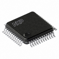
UCB1400BE,151 NXP Semiconductors, UCB1400BE,151 Datasheet - Page 31

UCB1400BE,151
Manufacturer Part Number
UCB1400BE,151
Description
IC AUDIO CODEC 3.3V 48-LQFP
Manufacturer
NXP Semiconductors
Type
Audio Codec '97r
Datasheet
1.UCB1400BEFE.pdf
(63 pages)
Specifications of UCB1400BE,151
Package / Case
48-LQFP
Data Interface
Serial
Resolution (bits)
20 b
Number Of Adcs / Dacs
2 / 2
Sigma Delta
No
S/n Ratio, Adcs / Dacs (db) Typ
97 / 91
Voltage - Supply, Analog
3 V ~ 3.6 V
Voltage - Supply, Digital
3 V ~ 3.6 V
Operating Temperature
-40°C ~ 85°C
Mounting Type
Surface Mount
Mounting Style
SMD/SMT
Lead Free Status / RoHS Status
Lead free / RoHS Compliant
Other names
935269304151
UCB1400BE-SNXP
UCB1400BE-SNXP
UCB1400BE-SNXP
UCB1400BE-SNXP
Available stocks
Company
Part Number
Manufacturer
Quantity
Price
Company:
Part Number:
UCB1400BE,151
Manufacturer:
NXP Semiconductors
Quantity:
10 000
Philips Semiconductors
9397 750 09611
Product data
11.1 On-chip reference circuit
When ASE is ‘1’, the ADC is started at a rising edge of the signal applied to the
ADCSYNC pin. In this mode, writing ‘1’ to the AS bit will arm the ADC, such that it will
start in the first detected rising edge of the ADCSYNC signal. A rising edge of the
signal connected to the ADCSYNC pin occurring during the tracking time is ignored;
the ADC conversion is started on the first rising edge detected after this delay time.
This mode is particularly useful when the internal ADC has to be synchronized to the
external system. Note that the AVE bit should not be set to ‘1’ when ASE is ‘1’.
The result of the conversion is stored in the ADC Data register (0x68), after the
completion of the conversion. An interrupt may be generated whenever a conversion
is completed (ADCP and/or ADCN bits in the Positive and Negative INT Enable
registers) to ease the synchronization between the UCB1400 and the system
controller. The ADV bit in the ADC Data register 0x68 indicates the status of the ADC
data; it equals ‘0’ when an ADC sequence is started, which implies that the ADC
result is not valid, and it equals ‘1’ when the ADC conversion is completed and the
result is stored in the ADC Data register (0x68).
The applied voltage on the four analog inputs of the UCB1400 (AD0-AD3) is
attenuated before it is applied to the ADC input multiplexer using on-chip resistive
dividers. These high voltage inputs are optimized to handle voltages larger than the
used supply voltage. The built-in resistive voltage dividers are only activated if the
corresponding analog input is selected. The resistive dividers are made floating when
the input is not selected by the ADC input multiplexer, such that the input leakage of
these high voltage analog pins is minimized. This makes these analog inputs very
suitable to monitor battery voltages.
The UCB1400 contains an on-chip reference voltage source, which generates the
reference voltage for the 10-bit ADC and touch screen bias. The internal bandgap
circuit is activated if the 10-bit ADC or touch screen function is activated. This
reduces the current consumption of the UCB1400 in standby mode.
The internal reference voltage is connected to the VREFBYP pin, where an external
capacitor can be connected to filter this reference voltage, if the VREFB bit (register
0x66) is set to ‘1’.
Fig 23. AD0-AD3 resistive dividers block diagram.
Rev. 02 — 21 June 2002
AD[n]
Audio codec with touch screen controller
INPUT
ADC
MUX
and power management monitor
SN00241
AI[2:0]
© Koninklijke Philips Electronics N.V. 2002. All rights reserved.
UCB1400
31 of 63


