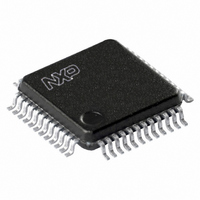
UCB1400BE,151 NXP Semiconductors, UCB1400BE,151 Datasheet - Page 16

UCB1400BE,151
Manufacturer Part Number
UCB1400BE,151
Description
IC AUDIO CODEC 3.3V 48-LQFP
Manufacturer
NXP Semiconductors
Type
Audio Codec '97r
Datasheet
1.UCB1400BEFE.pdf
(63 pages)
Specifications of UCB1400BE,151
Package / Case
48-LQFP
Data Interface
Serial
Resolution (bits)
20 b
Number Of Adcs / Dacs
2 / 2
Sigma Delta
No
S/n Ratio, Adcs / Dacs (db) Typ
97 / 91
Voltage - Supply, Analog
3 V ~ 3.6 V
Voltage - Supply, Digital
3 V ~ 3.6 V
Operating Temperature
-40°C ~ 85°C
Mounting Type
Surface Mount
Mounting Style
SMD/SMT
Lead Free Status / RoHS Status
Lead free / RoHS Compliant
Other names
935269304151
UCB1400BE-SNXP
UCB1400BE-SNXP
UCB1400BE-SNXP
UCB1400BE-SNXP
Available stocks
Company
Part Number
Manufacturer
Quantity
Price
Company:
Part Number:
UCB1400BE,151
Manufacturer:
NXP Semiconductors
Quantity:
10 000
Philips Semiconductors
9397 750 09611
Product data
8.5.1 SLOTREQ protocol
8.5 Variable sample rate signaling protocol
8.6 Wake-up support
The AC-link is defined for a fixed transfer rate of 48 kHz. To support the diverse
sample rates, UCB1400 implements the Variable Sample Rate Signaling Protocol of
the AC ’97 Component Specification :
To control the AC ’97 Controller to output a rate other than 48 kHz, the UCB1400
examines its sample rate control registers, the state of its FIFOs, and the incoming
SDATA_OUT tag bits at the beginning of each audio output frame to determine which
SLOTREQ bits to set active (LOW). SLOTREQ bits asserted during the current audio
input frame signal which active output slots require data from the AC ’97 Digital
Controller in the next audio output frame. An active output slot is defined as any slot
supported by UCB1400 that is not in a power-down state.
In case of UCB1400, the only SLOTREQ bits used are that for slot 3 and slot 4
request (bits 11 and 10 of input slot 1). SLOTREQ bits for all other slots shall be
stuffed with 0s by UCB1400. Note that although SLOTREQ bits reside in slot 1, their
validity does not depend on the tag bit for Valid Slot 1 Address (see also
Pressing the touch screen is an example of events that might need to wake-up the
host CPU that has suspended into a low power state.
power-down/power-up sequence. The UCB1400 powers down the AC Link
subsequent to its PR4 bit being programmed to 1. When enabled to wake on, e.g., a
touch screen event, a wake event causes the UCB1400 to transition IRQOUT from
LOW to HIGH. The system controller can use this information as a signal to wake up.
Subsequently, the first thing that the device driver must do to reestablish
communications with the UCB1400 is to command the AC ’97 Digital Controller to
execute a warm reset to the AC Link. Alternatively, if the GIEN bit in the Feature
CSR1 register (0x6A) is set, a wake event will cause the UCB1400 to transition its
SDATA_IN from LOW to HIGH. The UCB1400 shall keep SDATA_IN HIGH until it has
sampled SYNC having gone HIGH, and then LOW.
•
•
To control the AC ’97 Controller to input a rate other than 48 kHz, the UCB1400
uses the tag bit for slot 3 and 4 (PCM L & R) to indicate whether valid data is
present or not.
To control the AC ’97 Controller to output a rate other than 48 kHz, the UCB1400
uses the active-low SLOTREQ bit for slot 3 and slot 4 (PCM L & R) to indicate
whether it needs data from the AC ’97 Controller.
Rev. 02 — 21 June 2002
Audio codec with touch screen controller
and power management monitor
Figure 11
© Koninklijke Philips Electronics N.V. 2002. All rights reserved.
shows the AC Link
UCB1400
Section
16 of 63
8.4).


