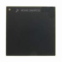
MC68EC060RC50 Freescale Semiconductor, MC68EC060RC50 Datasheet - Page 50

MC68EC060RC50
Manufacturer Part Number
MC68EC060RC50
Description
IC MPU 32BIT 50MHZ 206-PGA
Manufacturer
Freescale Semiconductor
Specifications of MC68EC060RC50
Processor Type
M680x0 32-Bit
Speed
50MHz
Voltage
3.3V
Mounting Type
Surface Mount
Package / Case
206-PGA
Family Name
M68000
Device Core
ColdFire
Device Core Size
32b
Frequency (max)
50MHz
Instruction Set Architecture
RISC
Supply Voltage 1 (typ)
3.3V
Operating Supply Voltage (max)
3.465V
Operating Supply Voltage (min)
3.135V
Operating Temp Range
0C to 110C
Operating Temperature Classification
Commercial
Mounting
Through Hole
Pin Count
206
Package Type
PGA
Lead Free Status / RoHS Status
Contains lead / RoHS non-compliant
Features
-
Lead Free Status / Rohs Status
Compliant
Available stocks
Company
Part Number
Manufacturer
Quantity
Price
Company:
Part Number:
MC68EC060RC50
Manufacturer:
NXP
Quantity:
1 746
- Current page: 50 of 416
- Download datasheet (2Mb)
Signal Description
nals are examined to determine whether the processor should invalidate matching cache
entries to maintain cache coherency.
2.1.2 Cycle Long-Word Address (CLA)
This active-low input signal controls the operation of A3 and A2 during bus cycles. Following
each clock-enabled clock edge in which CLA is asserted, the long-word address for each of
the four transfers encoded on A3 and A2 will increment in a circular wraparound fashion. If
CLA is negated during a clock-enabled clock edge, the values on A3 and A2 will not change.
It is not necessary to synchronize CLA with TA.
2.2 DATA BUS (D31–D0)
These three-state bidirectional signals provide the general-purpose data path between the
MC68060 and all other devices. The data bus can transfer 8, 16, or 32 bits of data per bus
transfer. During a burst bus cycle, the 128 bits of line information are transferred using four
32-bit transfers.
2.3 TRANSFER ATTRIBUTE SIGNALS
The following paragraphs describe the transfer attribute signals, which provide additional
information about the bus transfer cycle. Refer to Section 7 Bus Operation for detailed
information about the relationship of the transfer attribute signals to bus operation.
2.3.1 Transfer Cycle Type (TT1, TT0)
The processor drives these three-state signals to indicate the type of access for the current
bus cycle. During bus cycle transfers by an alternate bus master when the processor is
allowed to snoop bus transactions, TT1 is sampled. Only normal and MOVE16 accesses
can be snooped. Table 2-2 lists the definition of the TTx encoding. The acknowledge access
(TT1 = 1 and TT0 = 1) is used for interrupt acknowledge, breakpoint acknowledge, and low-
power stop broadcast bus cycles.
2.3.2 Transfer Cycle Modifier (TM2–TM0)
These three-state outputs provide supplemental information for each transfer cycle type.
Table 2-3 lists the encoding for normal (TTx = 00) and MOVE16 (TTx = 01) transfers, and
Table 2-4 lists the encoding for alternate access transfers (TTx = 10). For interrupt acknowl-
edge transfers, the TMx signals carry the interrupt level being acknowledged. For breakpoint
2-4
TT1
0
0
1
1
Table 2-2. Transfer-Type Encoding
TT0
0
1
0
1
M68060 USER’S MANUAL
Normal Access
MOVE16 Access
Alternate Logical Function Code Access, De-
bug Access
Acknowledge Access, Low-Power Stop
Broadcast
Transfer Type
MOTOROLA
Related parts for MC68EC060RC50
Image
Part Number
Description
Manufacturer
Datasheet
Request
R
Part Number:
Description:
Manufacturer:
Freescale Semiconductor, Inc
Datasheet:
Part Number:
Description:
Manufacturer:
Freescale Semiconductor, Inc
Datasheet:
Part Number:
Description:
Manufacturer:
Freescale Semiconductor, Inc
Datasheet:
Part Number:
Description:
Manufacturer:
Freescale Semiconductor, Inc
Datasheet:
Part Number:
Description:
Manufacturer:
Freescale Semiconductor, Inc
Datasheet:
Part Number:
Description:
Manufacturer:
Freescale Semiconductor, Inc
Datasheet:
Part Number:
Description:
Manufacturer:
Freescale Semiconductor, Inc
Datasheet:
Part Number:
Description:
Manufacturer:
Freescale Semiconductor, Inc
Datasheet:
Part Number:
Description:
Manufacturer:
Freescale Semiconductor, Inc
Datasheet:
Part Number:
Description:
Manufacturer:
Freescale Semiconductor, Inc
Datasheet:
Part Number:
Description:
Manufacturer:
Freescale Semiconductor, Inc
Datasheet:
Part Number:
Description:
Manufacturer:
Freescale Semiconductor, Inc
Datasheet:
Part Number:
Description:
Manufacturer:
Freescale Semiconductor, Inc
Datasheet:
Part Number:
Description:
Manufacturer:
Freescale Semiconductor, Inc
Datasheet:
Part Number:
Description:
Manufacturer:
Freescale Semiconductor, Inc
Datasheet:


