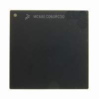
MC68EC060RC50 Freescale Semiconductor, MC68EC060RC50 Datasheet - Page 100

MC68EC060RC50
Manufacturer Part Number
MC68EC060RC50
Description
IC MPU 32BIT 50MHZ 206-PGA
Manufacturer
Freescale Semiconductor
Specifications of MC68EC060RC50
Processor Type
M680x0 32-Bit
Speed
50MHz
Voltage
3.3V
Mounting Type
Surface Mount
Package / Case
206-PGA
Family Name
M68000
Device Core
ColdFire
Device Core Size
32b
Frequency (max)
50MHz
Instruction Set Architecture
RISC
Supply Voltage 1 (typ)
3.3V
Operating Supply Voltage (max)
3.465V
Operating Supply Voltage (min)
3.135V
Operating Temp Range
0C to 110C
Operating Temperature Classification
Commercial
Mounting
Through Hole
Pin Count
206
Package Type
PGA
Lead Free Status / RoHS Status
Contains lead / RoHS non-compliant
Features
-
Lead Free Status / Rohs Status
Compliant
Available stocks
Company
Part Number
Manufacturer
Quantity
Price
Company:
Part Number:
MC68EC060RC50
Manufacturer:
NXP
Quantity:
1 746
- Current page: 100 of 416
- Download datasheet (2Mb)
SECTION 5
CACHES
The MC68060 contains two independent 8-Kbyte, on-chip caches which can be accessed
simultaneously for instruction and operand data. The caches improve system performance
by providing low latency data to the MC68060 instruction and data pipes. This decouples
processor performance from system memory performance and increases bus availability for
alternate bus masters.
As shown in Figure 5-1, the instruction and data caches are contained in the instruction and
data memory units. The appropriate memory unit independently services instruction
prefetch from the instruction fetch unit (IFU) and data requests from the operand pipe unit
(OPU). The memory units translate the logical address in parallel with indexing into the
cache. If the translated (physical) address matches one of the cache entries, the access hits
in the cache. For a read operation, the memory unit supplies the data to the IPU instruction
buffer or the OPU, and for a write operation, the memory unit updates the cache. If the
access does not match one of the cache entries (misses in the cache) or a write access must
be written through to memory, the appropriate memory unit sends an external bus request
to the bus controller. The bus controller then reads or writes the required data. In the event
that the bus controller receives an external bus request from both memory units, the bus
controller invokes its priority scheme to choose between IPU and OPU requests.
To maintain cache coherency, the MC68060 provides automatic snoop-invalidation when it
is not the bus master. Unlike the MC68040, the MC68060 cannot not source or sink cache
data during alternate bus master accesses.
The MC68060 implements a bus snooper that maintains cache coherency by monitoring an
alternate bus master access to memory and invalidating matching cache lines during the
alternate bus master access. The MC68060 requires that memory pages shared with other
bus masters be cache inhibited or marked cachable writethrough (instead of copyback).
When a processor writes to writethrough pages, external memory is always updated through
an external bus access after updating the cache, keeping memory and cached data consis-
tent.
5.1 CACHE OPERATION
Both four-way set-associative caches have 128 sets of four 16-byte lines. Each set in both
caches has a tag (consisting of the upper 21 bits of the physical address), status information,
and four long words (128 bits) of data. The status information for the instruction cache is a
single valid bit for the line. The status information for the data cache is a valid bit and a dirty
MOTOROLA
M68060 USER’S MANUAL
5-1
Related parts for MC68EC060RC50
Image
Part Number
Description
Manufacturer
Datasheet
Request
R
Part Number:
Description:
Manufacturer:
Freescale Semiconductor, Inc
Datasheet:
Part Number:
Description:
Manufacturer:
Freescale Semiconductor, Inc
Datasheet:
Part Number:
Description:
Manufacturer:
Freescale Semiconductor, Inc
Datasheet:
Part Number:
Description:
Manufacturer:
Freescale Semiconductor, Inc
Datasheet:
Part Number:
Description:
Manufacturer:
Freescale Semiconductor, Inc
Datasheet:
Part Number:
Description:
Manufacturer:
Freescale Semiconductor, Inc
Datasheet:
Part Number:
Description:
Manufacturer:
Freescale Semiconductor, Inc
Datasheet:
Part Number:
Description:
Manufacturer:
Freescale Semiconductor, Inc
Datasheet:
Part Number:
Description:
Manufacturer:
Freescale Semiconductor, Inc
Datasheet:
Part Number:
Description:
Manufacturer:
Freescale Semiconductor, Inc
Datasheet:
Part Number:
Description:
Manufacturer:
Freescale Semiconductor, Inc
Datasheet:
Part Number:
Description:
Manufacturer:
Freescale Semiconductor, Inc
Datasheet:
Part Number:
Description:
Manufacturer:
Freescale Semiconductor, Inc
Datasheet:
Part Number:
Description:
Manufacturer:
Freescale Semiconductor, Inc
Datasheet:
Part Number:
Description:
Manufacturer:
Freescale Semiconductor, Inc
Datasheet:


