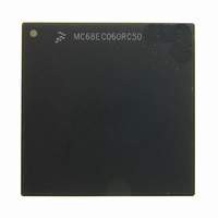
MC68EC060RC50 Freescale Semiconductor, MC68EC060RC50 Datasheet - Page 186

MC68EC060RC50
Manufacturer Part Number
MC68EC060RC50
Description
IC MPU 32BIT 50MHZ 206-PGA
Manufacturer
Freescale Semiconductor
Specifications of MC68EC060RC50
Processor Type
M680x0 32-Bit
Speed
50MHz
Voltage
3.3V
Mounting Type
Surface Mount
Package / Case
206-PGA
Family Name
M68000
Device Core
ColdFire
Device Core Size
32b
Frequency (max)
50MHz
Instruction Set Architecture
RISC
Supply Voltage 1 (typ)
3.3V
Operating Supply Voltage (max)
3.465V
Operating Supply Voltage (min)
3.135V
Operating Temp Range
0C to 110C
Operating Temperature Classification
Commercial
Mounting
Through Hole
Pin Count
206
Package Type
PGA
Lead Free Status / RoHS Status
Contains lead / RoHS non-compliant
Features
-
Lead Free Status / Rohs Status
Compliant
Available stocks
Company
Part Number
Manufacturer
Quantity
Price
Company:
Part Number:
MC68EC060RC50
Manufacturer:
NXP
Quantity:
1 746
- Current page: 186 of 416
- Download datasheet (2Mb)
Clock Idle (CI)
Clock 3 (C3)
Clock 4 (C4)
7.7.6 Emulating CAS2 and CAS Misaligned
The CAS2 and CAS (with misaligned operands) are not supported in hardware by the
MC68060. If these instructions are encountered, an unimplemented integer exception is
taken. Once the opcode for a CAS2 or CAS is decoded, the MOVEC instruction to the
MOTOROLA
When the processor recognizes TA at the end of the last read transfer for the locked bus
cycle, it negates TIP during the first half of the next clock.
The processor does not assert any new control signals during the idle clock states, but it
may begin the modify portion of the sequence at this time. The R/W signal remains in the
read mode until C3 to prevent bus conflicts with the preceding read portion of the cycle
and the data bus is not driven until C4.
During C3, the processor places valid values on the address bus and transfer attributes
and drives R/W low for a write cycle. The processor asserts TS to indicate the beginning
of a bus cycle. The TIP signal is also asserted at this time to indicate that a bus cycle is
active. LOCKE is asserted during C3 for the last write bus cycle of the locked sequence.
If multiple write transfers are required for misaligned operands or multiple operands,
LOCKE is asserted only for the final write transfer.
The processor pre-conditions the data bus during C3 to improve AC timing. The process
of pre-conditioning involves reinforcing the logic level that is already at the data pin. If the
voltage level is originally zero volts, nothing is done; if the voltage level is 3.3 V, that volt-
age level is reinforced; however, if the voltage level is originally 5 V, the processor drives
that data pin from 5 V down to 3.3 V. Note that no active logic change is done at this time.
The actual logic level change is done in C4. This pre-conditioning affects operation prima-
rily when using the processor in a 5-V system.
During C4, the processor negates TS and drives the appropriate bytes of the data bus with
the data to be written. All other bytes are driven with undefined values. The selected de-
vice uses R/W, SIZ1, SIZ0, A1, and A0 or BSx, to register the information on the data bus.
Any or all of the data bus bytes (D31–D24, D23–D16, D15–D8, and D7–D0) are selected
by SIZ1, SIZ0, A1, and A0 or BSx. Concurrently, the selected device asserts TA. Assum-
ing that the acknowledge termination ignore state capability is disabled, the processor
samples the level of TA; if TA is asserted, the bus cycle terminates. If TA is not recognized
asserted at the end of C4, the processor appends a wait state instead of terminating the
transfer. The processor continues to sample the TA signal on successive rising edges of
BCLK until it is recognized asserted.
When the processor recognizes TA at the rising edge of BCLK, the bus cycle is terminat-
ed, but TIP remains asserted if the processor is ready to begin another bus cycle. Other-
wise, the processor negates TIP during the next clock. The processor also three-states
the data bus during the next clock following termination of the write cycle. When the last
write transfer is terminated, LOCKE is negated. The processor also negates LOCK if the
next bus cycle is not a read-modify-write operation.
M68060 USER’S MANUAL
Bus Operation
7-31
Related parts for MC68EC060RC50
Image
Part Number
Description
Manufacturer
Datasheet
Request
R
Part Number:
Description:
Manufacturer:
Freescale Semiconductor, Inc
Datasheet:
Part Number:
Description:
Manufacturer:
Freescale Semiconductor, Inc
Datasheet:
Part Number:
Description:
Manufacturer:
Freescale Semiconductor, Inc
Datasheet:
Part Number:
Description:
Manufacturer:
Freescale Semiconductor, Inc
Datasheet:
Part Number:
Description:
Manufacturer:
Freescale Semiconductor, Inc
Datasheet:
Part Number:
Description:
Manufacturer:
Freescale Semiconductor, Inc
Datasheet:
Part Number:
Description:
Manufacturer:
Freescale Semiconductor, Inc
Datasheet:
Part Number:
Description:
Manufacturer:
Freescale Semiconductor, Inc
Datasheet:
Part Number:
Description:
Manufacturer:
Freescale Semiconductor, Inc
Datasheet:
Part Number:
Description:
Manufacturer:
Freescale Semiconductor, Inc
Datasheet:
Part Number:
Description:
Manufacturer:
Freescale Semiconductor, Inc
Datasheet:
Part Number:
Description:
Manufacturer:
Freescale Semiconductor, Inc
Datasheet:
Part Number:
Description:
Manufacturer:
Freescale Semiconductor, Inc
Datasheet:
Part Number:
Description:
Manufacturer:
Freescale Semiconductor, Inc
Datasheet:
Part Number:
Description:
Manufacturer:
Freescale Semiconductor, Inc
Datasheet:


