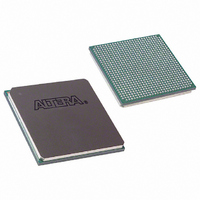
EP1S20F780C7 Altera, EP1S20F780C7 Datasheet - Page 49

EP1S20F780C7
Manufacturer Part Number
EP1S20F780C7
Description
IC STRATIX FPGA 20K LE 780-FBGA
Manufacturer
Altera
Series
Stratix®r
Datasheet
1.EP1S10F780C7.pdf
(276 pages)
Specifications of EP1S20F780C7
Number Of Logic Elements/cells
18460
Number Of Labs/clbs
1846
Total Ram Bits
1669248
Number Of I /o
586
Voltage - Supply
1.425 V ~ 1.575 V
Mounting Type
Surface Mount
Operating Temperature
0°C ~ 85°C
Package / Case
780-FBGA
Family Name
Stratix
Number Of Logic Blocks/elements
18460
# I/os (max)
586
Frequency (max)
420.17MHz
Process Technology
0.13um (CMOS)
Operating Supply Voltage (typ)
1.5V
Logic Cells
18460
Ram Bits
1669248
Operating Supply Voltage (min)
1.425V
Operating Supply Voltage (max)
1.575V
Operating Temp Range
0C to 85C
Operating Temperature Classification
Commercial
Mounting
Surface Mount
Pin Count
780
Package Type
FC-FBGA
Lead Free Status / RoHS Status
Contains lead / RoHS non-compliant
Number Of Gates
-
Lead Free Status / Rohs Status
Not Compliant
Other names
544-1116
Available stocks
Company
Part Number
Manufacturer
Quantity
Price
Company:
Part Number:
EP1S20F780C7
Manufacturer:
ALTERA
Quantity:
1 238
Company:
Part Number:
EP1S20F780C7
Manufacturer:
ALTERA
Quantity:
453
Company:
Part Number:
EP1S20F780C7L
Manufacturer:
NXP
Quantity:
1 448
Company:
Part Number:
EP1S20F780C7N
Manufacturer:
ALTERA
Quantity:
3 000
Altera Corporation
July 2005
The read and write operation of the memory is controlled by the WREN
signal, which sets the ports into either read or write modes. There is no
separate read enable (RE) signal.
Writing into RAM is controlled by both the WREN and byte enable
(byteena) signals for each port. The default value for the byteena
signal is high, in which case writing is controlled only by the WREN signal.
The byte enables are available for the ×18, ×36, and ×72 modes. In the
×144 simple dual-port mode, the two sets of byteena signals
(byteena_a and byteena_b) are combined to form the necessary
16 byte enables.
64K
32K
16K
8K
Table 2–9. M-RAM Block Configurations (True Dual-Port)
Table 2–10. Byte Enable for M-RAM Blocks
byteena[3..0]
×
×
×
×
72
[0] = 1
[1] = 1
[2] = 1
[3] = 1
[4] = 1
[5] = 1
[6] = 1
[7] = 1
9
18
36
Port A
Tables 2–10
datain ×18
[17..9]
64K × 9
[8..0]
–
–
–
–
–
–
v
v
v
v
and
2–11
32K × 18
summarize the byte selection.
Stratix Device Handbook, Volume 1
v
v
v
v
datain ×36
Notes
[26..18]
[35..27]
[17..9]
[8..0]
Port B
–
–
–
–
(1),
16K × 36
(2)
v
v
v
v
Stratix Architecture
datain ×72
[26..18]
[35..27]
[44..36]
[53..45]
[62..54]
[71..63]
[17..9]
[8..0]
8K × 72
v
v
v
v
2–35


