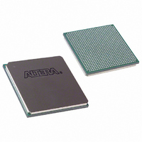
EP1S20F780C7 Altera, EP1S20F780C7 Datasheet - Page 102

EP1S20F780C7
Manufacturer Part Number
EP1S20F780C7
Description
IC STRATIX FPGA 20K LE 780-FBGA
Manufacturer
Altera
Series
Stratix®r
Datasheet
1.EP1S10F780C7.pdf
(276 pages)
Specifications of EP1S20F780C7
Number Of Logic Elements/cells
18460
Number Of Labs/clbs
1846
Total Ram Bits
1669248
Number Of I /o
586
Voltage - Supply
1.425 V ~ 1.575 V
Mounting Type
Surface Mount
Operating Temperature
0°C ~ 85°C
Package / Case
780-FBGA
Family Name
Stratix
Number Of Logic Blocks/elements
18460
# I/os (max)
586
Frequency (max)
420.17MHz
Process Technology
0.13um (CMOS)
Operating Supply Voltage (typ)
1.5V
Logic Cells
18460
Ram Bits
1669248
Operating Supply Voltage (min)
1.425V
Operating Supply Voltage (max)
1.575V
Operating Temp Range
0C to 85C
Operating Temperature Classification
Commercial
Mounting
Surface Mount
Pin Count
780
Package Type
FC-FBGA
Lead Free Status / RoHS Status
Contains lead / RoHS non-compliant
Number Of Gates
-
Lead Free Status / Rohs Status
Not Compliant
Other names
544-1116
Available stocks
Company
Part Number
Manufacturer
Quantity
Price
Company:
Part Number:
EP1S20F780C7
Manufacturer:
ALTERA
Quantity:
1 238
Company:
Part Number:
EP1S20F780C7
Manufacturer:
ALTERA
Quantity:
453
Company:
Part Number:
EP1S20F780C7L
Manufacturer:
NXP
Quantity:
1 448
Company:
Part Number:
EP1S20F780C7N
Manufacturer:
ALTERA
Quantity:
3 000
PLLs & Clock Networks
2–88
Stratix Device Handbook, Volume 1
Clock Multiplication & Division
Each Stratix device enhanced PLL provides clock synthesis for PLL
output ports using m/(n × post-scale counter) scaling factors. The input
clock is divided by a pre-scale divider, n, and is then multiplied by the m
feedback factor. The control loop drives the VCO to match f
Each output port has a unique post-scale counter that divides down the
high-frequency VCO. For multiple PLL outputs with different
frequencies, the VCO is set to the least common multiple of the output
frequencies that meets its frequency specifications. Then, the post-scale
dividers scale down the output frequency for each output port. For
example, if output frequencies required from one PLL are 33 and 66 MHz,
set the VCO to 330 MHz (the least common multiple in the VCO’s range).
There is one pre-scale counter, n, and one multiply counter, m, per PLL,
with a range of 1 to 512 on each. There are two post-scale counters (l) for
regional clock output ports, four counters (g) for global clock output
ports, and up to four counters (e) for external clock outputs, all ranging
from 1 to 1024 with a 50% duty cycle setting. The post-scale counters
range from 1 to 512 with any non-50% duty cycle setting. The Quartus II
software automatically chooses the appropriate scaling factors according
to the input frequency, multiplication, and division values entered.
Clock Switchover
To effectively develop high-reliability network systems, clocking schemes
must support multiple clocks to provide redundancy. For this reason,
Stratix device enhanced PLLs support a flexible clock switchover
capability.
circuit.The switchover circuit is configurable, so you can define how to
implement it. Clock-sense circuitry automatically switches from the
primary to secondary clock for PLL reference when the primary clock
signal is not present.
Figure 2–53
shows a block diagram of the switchover
Altera Corporation
IN
× (m/n).
July 2005


