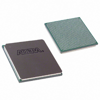
EP1S20F780C7 Altera, EP1S20F780C7 Datasheet - Page 245

EP1S20F780C7
Manufacturer Part Number
EP1S20F780C7
Description
IC STRATIX FPGA 20K LE 780-FBGA
Manufacturer
Altera
Series
Stratix®r
Datasheet
1.EP1S10F780C7.pdf
(276 pages)
Specifications of EP1S20F780C7
Number Of Logic Elements/cells
18460
Number Of Labs/clbs
1846
Total Ram Bits
1669248
Number Of I /o
586
Voltage - Supply
1.425 V ~ 1.575 V
Mounting Type
Surface Mount
Operating Temperature
0°C ~ 85°C
Package / Case
780-FBGA
Family Name
Stratix
Number Of Logic Blocks/elements
18460
# I/os (max)
586
Frequency (max)
420.17MHz
Process Technology
0.13um (CMOS)
Operating Supply Voltage (typ)
1.5V
Logic Cells
18460
Ram Bits
1669248
Operating Supply Voltage (min)
1.425V
Operating Supply Voltage (max)
1.575V
Operating Temp Range
0C to 85C
Operating Temperature Classification
Commercial
Mounting
Surface Mount
Pin Count
780
Package Type
FC-FBGA
Lead Free Status / RoHS Status
Contains lead / RoHS non-compliant
Number Of Gates
-
Lead Free Status / Rohs Status
Not Compliant
Other names
544-1116
Available stocks
Company
Part Number
Manufacturer
Quantity
Price
Company:
Part Number:
EP1S20F780C7
Manufacturer:
ALTERA
Quantity:
1 238
Company:
Part Number:
EP1S20F780C7
Manufacturer:
ALTERA
Quantity:
453
Company:
Part Number:
EP1S20F780C7L
Manufacturer:
NXP
Quantity:
1 448
Company:
Part Number:
EP1S20F780C7N
Manufacturer:
ALTERA
Quantity:
3 000
Altera Corporation
January 2006
Note to
(1)
Note to
(1)
Note to
(1)
Drive Strength
VCCIO Voltage
Level
Table 4–111. Output Delay Adder for Loading on LVTTL/LVCMOS Output Buffers
Table 4–112. Output Delay Adder for Loading on SSTL/HSTL Output Buffers
Table 4–113. Output Delay Adder for Loading on GTL+/GTL/CTT/PCI Output Buffers
Parameter
Parameter
The timing information in this table is preliminary.
The timing information in this table is preliminary.
The timing information in this table is preliminary.
Table
Table
Table
Conditions
Class II
Conditions
Class I
Conditions
4–111:
4–112:
4–113:
Value
3.3V
2.5V
Value
24mA
16mA
12mA
8mA
4mA
2mA
The scaling factors for column output pin timing in
are shown in units of time per pF unit of capacitance (ps/pF). Add this
delay to the t
pins in addition to the I/O adder delays shown in
4–108
3.3-V LVTTL
SSTL-3
and the IOE programmable delays in
GTL+
25
25
18
15
15
25
30
50
60
–
CO
or combinatorial timing path for output or bidirectional
2.5-V LVTTL
Output Pin Adder Delay (ps/pF)
GTL
18
18
Output Pin Adder Delay (ps/pF)
SSTL-2
Output Pin Adder Delay (ps/pF)
18
25
35
75
–
–
25
20
1.8-V LVTTL
CTT
120
25
25
40
-
–
–
–
Stratix Device Handbook, Volume 1
SSTL-1.8
DC & Switching Characteristics
25
25
Tables 4–109
Note (1)
1.5-V LVTTL
Note (1)
Tables 4–103
160
Tables 4–111
PCI
35
80
20
–
–
-
-
Note (1)
and 4–110.
1.5-V HSTL
25
20
LVCMOS
through
to
AGP
15
20
30
60
8
–
20
-
4–113
4–75


