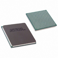
EP1S20F780C7 Altera, EP1S20F780C7 Datasheet - Page 109

EP1S20F780C7
Manufacturer Part Number
EP1S20F780C7
Description
IC STRATIX FPGA 20K LE 780-FBGA
Manufacturer
Altera
Series
Stratix®r
Datasheet
1.EP1S10F780C7.pdf
(276 pages)
Specifications of EP1S20F780C7
Number Of Logic Elements/cells
18460
Number Of Labs/clbs
1846
Total Ram Bits
1669248
Number Of I /o
586
Voltage - Supply
1.425 V ~ 1.575 V
Mounting Type
Surface Mount
Operating Temperature
0°C ~ 85°C
Package / Case
780-FBGA
Family Name
Stratix
Number Of Logic Blocks/elements
18460
# I/os (max)
586
Frequency (max)
420.17MHz
Process Technology
0.13um (CMOS)
Operating Supply Voltage (typ)
1.5V
Logic Cells
18460
Ram Bits
1669248
Operating Supply Voltage (min)
1.425V
Operating Supply Voltage (max)
1.575V
Operating Temp Range
0C to 85C
Operating Temperature Classification
Commercial
Mounting
Surface Mount
Pin Count
780
Package Type
FC-FBGA
Lead Free Status / RoHS Status
Contains lead / RoHS non-compliant
Number Of Gates
-
Lead Free Status / Rohs Status
Not Compliant
Other names
544-1116
Available stocks
Company
Part Number
Manufacturer
Quantity
Price
Company:
Part Number:
EP1S20F780C7
Manufacturer:
ALTERA
Quantity:
1 238
Company:
Part Number:
EP1S20F780C7
Manufacturer:
ALTERA
Quantity:
453
Company:
Part Number:
EP1S20F780C7L
Manufacturer:
NXP
Quantity:
1 448
Company:
Part Number:
EP1S20F780C7N
Manufacturer:
ALTERA
Quantity:
3 000
Figure 2–56. External Clock Outputs for Enhanced PLLs 11 & 12
Note to
(1)
Altera Corporation
July 2005
Counter
g 0
For PLL 11, this pin is CLK13n; for PLL 12 this pin is CLK7n.
Figure
From Internal
Logic or IOE
2–56:
Enhanced PLLs 11 and 12 support one single-ended output each (see
Figure
Therefore, to minimize jitter, do not place switching I/O pins next to this
output pin.
Stratix devices can drive any enhanced PLL driven through the global
clock or regional clock network to any general I/O pin as an external
output clock. The jitter on the output clock is not guaranteed for these
cases.
1.5-V HSTL Class II
1.8-V HSTL Class I
1.8-V HSTL Class II
SSTL-18 Class I
SSTL-18 Class II
SSTL-2 Class I
SSTL-2 Class II
SSTL-3 Class I
SSTL-3 Class II
AGP (1× and 2× )
CTT
Table 2–20. I/O Standards Supported for Enhanced PLL Pins (Part 2 of 2)
2–56). These outputs do not have their own VCC and GND signals.
I/O Standard
INCLK
v
v
v
v
v
v
v
v
v
v
v
Stratix Device Handbook, Volume 1
FBIN
v
v
v
v
v
v
v
v
v
v
v
Input
or CLK6n, I/O, PLL12_OUT (1)
PLLENABLE
CLK13n, I/O, PLL11_OUT
Stratix Architecture
EXTCLK
Output
v
v
v
v
v
v
v
v
v
v
v
2–95


