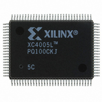
XC4005L-5PQ100C Xilinx Inc, XC4005L-5PQ100C Datasheet - Page 51

XC4005L-5PQ100C
Manufacturer Part Number
XC4005L-5PQ100C
Description
IC 3.3V FPGA 196 CLB'S 100-PQFP
Manufacturer
Xilinx Inc
Series
XC4000r
Datasheet
1.XC4005L-5PC84C.pdf
(175 pages)
Specifications of XC4005L-5PQ100C
Number Of Logic Elements/cells
466
Number Of Labs/clbs
196
Total Ram Bits
6272
Number Of I /o
77
Number Of Gates
5000
Voltage - Supply
3 V ~ 3.6 V
Mounting Type
Surface Mount
Operating Temperature
0°C ~ 85°C
Package / Case
100-BQFP
Lead Free Status / RoHS Status
Contains lead / RoHS non-compliant
Other names
122-1121
Available stocks
Company
Part Number
Manufacturer
Quantity
Price
chronous mode, an externally supplied clock input to CCLK
serializes the data.
Slave Serial Mode
In Slave Serial mode, the FPGA receives serial configura-
tion data on the rising edge of CCLK and, after loading its
configuration, passes additional data out, resynchronized
on the next falling edge of CCLK.
Multiple slave devices with identical configurations can be
wired with parallel DIN inputs. In this way, multiple devices
can be configured simultaneously.
Serial Daisy Chain
Multiple devices with different configurations can be con-
nected together in a “daisy chain,” and a single combined
bitstream used to configure the chain of slave devices.
To configure a daisy chain of devices, wire the CCLK pins
of all devices in parallel, as shown in
Connect the DOUT of each device to the DIN of the next.
The lead or master FPGA and following slaves each
passes resynchronized configuration data coming from a
single source. The header data, including the length count,
is passed through and is captured by each FPGA when it
recognizes the 0010 preamble. Following the length-count
data, each FPGA outputs a High on DOUT until it has
received its required number of data frames.
After an FPGA has received its configuration data, it
passes on any additional frame start bits and configuration
data on DOUT. When the total number of configuration
clocks applied after memory initialization equals the value
of the 24-bit length count, the FPGAs begin the start-up
sequence and become operational together. FPGA I/O are
normally released two CCLK cycles after the last configura-
tion bit is received.
up timing for an XC4000-Series device.
The daisy-chained bitstream is not simply a concatenation
of the individual bitstreams. The MakePROM program
must be used to combine the bitstreams for a daisy-
chained configuration.
Multi-Family Daisy Chain
All Xilinx FPGAs of the XC2000, XC3000, and XC4000
Series use a compatible bitstream format and can, there-
fore, be connected in a daisy chain in an arbitrary
sequence. There is, however, one limitation. The lead
device must belong to the highest family in the chain. If the
chain contains XC4000-Series devices, the master nor-
mally cannot be an XC2000 or XC3000 device.
The reason for this rule is shown in
Since all devices in the chain store the same length count
value and generate or receive one common sequence of
CCLK pulses, they all recognize length-count match on the
same CCLK edge, as indicated on the left edge of
Figure
September 18, 1996 (Version 1.04)
49. The master device then generates additional
Figure 49 on page 61
Figure 49 on page
Figure 55 on page
shows the start-
68.
61.
CCLK pulses until it reaches its finish point F. The different
families generate or require different numbers of additional
CCLK pulses until they reach F. Not reaching F means that
the device does not really finish its configuration, although
DONE may have gone High, the outputs became active,
and the internal reset was released. For the XC4000-
Series device, not reaching F means that readback cannot
be initiated and most boundary scan instructions cannot be
used.
The user has some control over the relative timing of these
events and can, therefore, make sure that they occur at the
proper time and the finish point F is reached. Timing is con-
trolled using MakeBits options.
XC3000 Master with an XC4000-Series Slave
Some designers want to use an inexpensive lead device in
peripheral mode and have the more precious I/O pins of the
XC4000-Series devices all available for user I/O.
provides a solution for that case.
This solution requires one CLB, one IOB and pin, and an
internal oscillator with a frequency of up to 5 MHz as a
clock source. The XC3000 master device must be config-
ured with late Internal Reset, which is the default option.
One CLB and one IOB in the lead XC3000-family device
are used to generate the additional CCLK pulse required by
the XC4000-Series devices.
removes the internal RESET signal, the 2-bit shift register
responds to its clock input and generates an active Low
output signal for the duration of the subsequent clock
period. An external connection between this output and
CCLK thus creates the extra CCLK pulse.
Express Mode (XC4000EX only)
Express mode is similar to Slave Serial mode, except the
data is presented in parallel format, and is clocked into the
target device a byte at a time rather than a bit at a time. The
data is loaded in parallel into eight different columns: it is
not internally serialized. Eight bits of configuration data are
loaded with every CCLK cycle, therefore this configuration
Figure 46: CCLK Generation for XC3000 Master
Driving an XC4000-Series Slave
0
1
1
0
0
Reset
.
.
etc
0
0
1
1
1
.
.
Active Low Output
Active High Output
When the lead device
OE/T
Output
Connected
to CCLK
Figure 46
X5223
4-55


