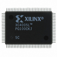
XC4005L-5PQ100C Xilinx Inc, XC4005L-5PQ100C Datasheet - Page 50

XC4005L-5PQ100C
Manufacturer Part Number
XC4005L-5PQ100C
Description
IC 3.3V FPGA 196 CLB'S 100-PQFP
Manufacturer
Xilinx Inc
Series
XC4000r
Datasheet
1.XC4005L-5PC84C.pdf
(175 pages)
Specifications of XC4005L-5PQ100C
Number Of Logic Elements/cells
466
Number Of Labs/clbs
196
Total Ram Bits
6272
Number Of I /o
77
Number Of Gates
5000
Voltage - Supply
3 V ~ 3.6 V
Mounting Type
Surface Mount
Operating Temperature
0°C ~ 85°C
Package / Case
100-BQFP
Lead Free Status / RoHS Status
Contains lead / RoHS non-compliant
Other names
122-1121
Available stocks
Company
Part Number
Manufacturer
Quantity
Price
XC4000 Series Field Programmable Gate Arrays
Configuration
Configuration is the process of loading design-specific pro-
gramming data into one or more FPGAs to define the func-
tional
interconnections. This is somewhat like loading the com-
mand registers of a programmable peripheral chip.
XC4000-Series devices use several hundred bits of config-
uration data per CLB and its associated interconnects.
Each configuration bit defines the state of a static memory
cell that controls either a function look-up table bit, a multi-
plexer input, or an interconnect pass transistor. The XACT-
step development system translates the design into a
netlist file. It automatically partitions, places and routes the
logic and generates the configuration data in PROM format.
Special Purpose Pins
Three configuration mode pins (M2, M1, M0) are sampled
prior to configuration to determine the configuration mode.
After configuration, these pins can be used as auxiliary
connections. M2 and M0 can be used as inputs, and M1
can be used as an output. The XACT step development
system does not use these resources unless they are
explicitly specified in the design entry. This is done by plac-
ing a special pad symbol called MD2, MD1, or MD0 instead
of the input or output pad symbol.
In XC4000-Series devices, the mode pins have weak pull-
up resistors during configuration. With all three mode pins
High, Slave Serial mode is selected, which is the most pop-
ular configuration mode. Therefore, for the most common
configuration mode, the mode pins can be left uncon-
nected. (Note, however, that the internal pull-up resistor
value can be as high as 100 k .) After configuration, these
pins can individually have weak pull-up or pull-down resis-
tors, as specified in the design. A pull-down resistor value
of 4.7 k is recommended.
These pins are located in the lower left chip corner and are
near the readback nets. This location allows convenient
routing if compatibility with the XC2000 and XC3000 family
conventions of M0/RT, M1/RD is desired.
Configuration Modes
XC4000E
XC4000EX devices have the same six modes, plus an
additional configuration mode. These modes are selected
by a 3-bit input code applied to the M2, M1, and M0 inputs.
There are three self-loading Master modes, two Peripheral
modes, and a Serial Slave mode, which is used primarily
for daisy-chained devices.
Express mode, is an additional slave mode that allows
high-speed parallel configuration of the high-capacity
XC4000EX devices. The coding for mode selection is
shown in
4-54
operation
Table
devices
20.
of
have
the
internal
six
The seventh mode, called
configuration
blocks
and
modes.
their
Table 20: Configuration Modes
Note:
A detailed description of each configuration mode, with tim-
ing information, is included later in this data sheet. During
configuration, some of the I/O pins are used temporarily for
the configuration process. All pins used during configura-
tion are shown in
Master Modes
The three Master modes use an internal oscillator to gener-
ate a Configuration Clock (CCLK) for driving potential slave
devices. They also generate address and timing for exter-
nal PROM(s) containing the configuration data.
Master Parallel (Up or Down) modes generate the CCLK
signal and PROM addresses and receive byte parallel data.
The data is internally serialized into the FPGA data-frame
format. The up and down selection generates starting
addresses at either zero or 3FFFF, for compatibility with dif-
ferent microprocessor addressing conventions. The Master
Serial mode generates CCLK and receives the configura-
tion data in serial form from a Xilinx serial-configuration
PROM.
CCLK speed is selectable as either 1 MHz (default) or 8
MHz (up to 10% lower for low-voltage devices). Configura-
tion always starts at the default slow frequency, then can
switch to the higher frequency during the first frame. Fre-
quency tolerance is -50% to +25%.
Peripheral Modes
The two Peripheral modes accept byte-wide data from a
bus. A RDY/BUSY status is available as a handshake sig-
nal. In Asynchronous Peripheral mode, the internal oscilla-
tor generates a CCLK burst signal that serializes the byte-
wide data. CCLK can also drive slave devices. In the syn-
Master Serial
Slave Serial
Master
Parallel Up
Master
Parallel Down
Peripheral
Synchronous*
Peripheral
Asynchronous
Express
(XC4000EX
only)
Reserved
Mode
* Peripheral Synchronous can be considered byte-
wide Slave Parallel
M2
Table 24 on page
0
1
1
1
0
1
0
0
M1
September 18, 1996 (Version 1.04)
0
1
0
1
1
0
1
0
M0
0
1
0
0
1
1
0
1
output
output
output
output
CCLK
input
input
input
78.
—
from 3FFFF
from 00000
Byte-Wide,
Byte-Wide,
decrement
Byte-Wide
Byte-Wide
Byte-Wide
increment
Bit-Serial
Bit-Serial
Data
—


