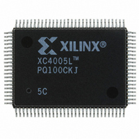
XC4005L-5PQ100C Xilinx Inc, XC4005L-5PQ100C Datasheet - Page 22

XC4005L-5PQ100C
Manufacturer Part Number
XC4005L-5PQ100C
Description
IC 3.3V FPGA 196 CLB'S 100-PQFP
Manufacturer
Xilinx Inc
Series
XC4000r
Datasheet
1.XC4005L-5PC84C.pdf
(175 pages)
Specifications of XC4005L-5PQ100C
Number Of Logic Elements/cells
466
Number Of Labs/clbs
196
Total Ram Bits
6272
Number Of I /o
77
Number Of Gates
5000
Voltage - Supply
3 V ~ 3.6 V
Mounting Type
Surface Mount
Operating Temperature
0°C ~ 85°C
Package / Case
100-BQFP
Lead Free Status / RoHS Status
Contains lead / RoHS non-compliant
Other names
122-1121
Available stocks
Company
Part Number
Manufacturer
Quantity
Price
XC4000 Series Field Programmable Gate Arrays
Optional Delay Guarantees Zero Hold Time
The data input to the register can optionally be delayed by
several nanoseconds. With the delay enabled, the setup
time of the input flip-flop is increased so that normal clock
routing does not result in a positive hold-time requirement.
A positive hold time requirement can lead to unreliable,
temperature- or processing-dependent operation.
The input flip-flop setup time is defined between the data
measured at the device I/O pin and the clock input at the
IOB (not at the clock pin). Any routing delay from the
device clock pin to the clock input of the IOB must, there-
fore, be subtracted from this setup time to arrive at the real
setup time requirement relative to the device pins. A short
specified setup time might, therefore, result in a negative
setup time at the device pins, i.e., a positive hold-time
requirement.
When a delay is inserted on the data line, more clock delay
can be tolerated without causing a positive hold-time
requirement. Sufficient delay eliminates the possibility of a
data hold-time requirement at the external pin. The maxi-
mum delay is therefore inserted as the default.
The XC4000E IOB has a one-tap delay element: either the
delay is inserted (default), or it is not. The delay guarantees
a zero hold time with respect to clocks routed through any
of the XC4000E global clock buffers. (See
and Buffers (XC4000E only)” on page 41
of the global clock buffers in the XC4000E.) For a shorter
input register setup time, with non-zero hold, attach a
NODELAY attribute or property to the flip-flop.
The XC4000EX IOB has a two-tap delay element, with
choices of a full delay, a partial delay, or no delay. The
attributes or properties used to select the desired delay are
shown in
MEDDELAY, and NODELAY. The default setting, with no
added attribute, ensures no hold time with respect to any of
the XC4000EX clock buffers, including the Global Low-
Skew buffers.
respect to the Global Early and FastCLK buffers. Inputs
with NODELAY may have a positive hold time with respect
to all clock buffers, including the FastCLK buffers. For a
description of each of these buffers, see
Buffers (XC4000EX only)” on page
Table 12: XC4000EX IOB Input Delay Element
4-26
full delay
(default, no
attribute added)
MEDDELAY
NODELAY
Value
Table
12. The choices are no added attribute,
MEDDELAY ensures no hold time with
Zero Hold with respect to Global Low-
Skew Buffer, Global Early Buffer, or
FastCLK Buffer
Zero Hold with respect to Global Early
Buffer or FastCLK Buffer
Short Setup, positive Hold time
When to Use
43.
“Global Nets and
for a description
“Global Nets
Additional Input Latch for Fast Capture (XC4000EX
only)
The XC4000EX IOB has an additional optional latch on the
input. This latch, as shown in
output clock — the clock used for the output flip-flop —
rather than the input clock. Therefore, two different clocks
can be used to clock the two input storage elements. This
additional latch allows the very fast capture of input data,
which is then synchronized to the internal clock by the IOB
flip-flop or latch.
To use this Fast Capture technique, drive the output clock
pin (the Fast Capture latching signal) from the output of one
of the Global Early or FastCLK buffers supplied in the
XC4000EX.
clocked by a Global Low-Skew buffer, to synchronize the
incoming data to the internal logic. (See
special buffers are described in
(XC4000EX only)” on page
The Fast Capture latch is designed primarily for use with a
Global Early buffer. For Fast Capture, a single clock signal
is routed through both a Global Early buffer and a Global
Low-Skew buffer. (The two buffers share an input pad.)
The Fast Capture latch is clocked by the Global Early
buffer, and the standard IOB flip-flop or latch is clocked by
the Global Low-Skew buffer. This mode is the safest way to
use the Fast Capture latch, because the clock buffers on
both storage elements are driven by the same pad. There
is no external skew between clock pads to create potential
problems.
Alternatively, a FastCLK buffer can be used to minimize the
setup time of device inputs, if a positive hold time is accept-
able. Use the FastCLK buffer to clock the Fast Capture
latch, and a slower clock buffer to clock the standard IOB
flip-flop or latch. Either the Global Early buffer or the Global
Low-Skew buffer can be used for the second storage ele-
Figure 18: Examples Using XC4000EX Fast
Capture Latch
IPAD
IPAD
IPAD
IPAD
IPAD
BUFFCLK
BUFGLS
BUFGE
BUFGLS
The second storage element should be
NODELAY
D
GF
D
GF
CE
C
CE
C
September 18, 1996 (Version 1.04)
ILFFX
ILFFX
43.
Figure
“Global Nets and Buffers
17, is clocked by the
Figure
Q
Q
18.) These
X6705
to internal
logic
to internal
logic


