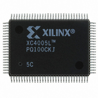
XC4005L-5PQ100C Xilinx Inc, XC4005L-5PQ100C Datasheet - Page 15

XC4005L-5PQ100C
Manufacturer Part Number
XC4005L-5PQ100C
Description
IC 3.3V FPGA 196 CLB'S 100-PQFP
Manufacturer
Xilinx Inc
Series
XC4000r
Datasheet
1.XC4005L-5PC84C.pdf
(175 pages)
Specifications of XC4005L-5PQ100C
Number Of Logic Elements/cells
466
Number Of Labs/clbs
196
Total Ram Bits
6272
Number Of I /o
77
Number Of Gates
5000
Voltage - Supply
3 V ~ 3.6 V
Mounting Type
Surface Mount
Operating Temperature
0°C ~ 85°C
Package / Case
100-BQFP
Lead Free Status / RoHS Status
Contains lead / RoHS non-compliant
Other names
122-1121
Available stocks
Company
Part Number
Manufacturer
Quantity
Price
Single-Port Level-Sensitive Timing Mode
Note: Edge-triggered mode is recommended for all new
designs. Level-sensitive mode, also called asynchronous
mode, is still supported for XC4000-Series backward-com-
patibility with the XC4000 family.
Level-sensitive RAM timing is simple in concept but can be
complicated in execution. Data and address signals are
presented, then a positive pulse on the write enable pin
(WE) performs a write into the RAM at the designated
address. As indicated by the “level-sensitive” label, this
RAM acts like a latch. During the WE High pulse, changing
the data lines results in new data written to the old address.
Changing the address lines while WE is High results in spu-
rious data written to the new address—and possibly at
other addresses as well, as the address lines inevitably do
not all change simultaneously.
The user must generate a carefully timed WE signal. The
delay on the WE signal and the address lines must be care-
fully verified to ensure that WE does not become active until
after the address lines have settled, and that WE goes inac-
tive before the address lines change again. The data must
be stable before and after the falling edge of WE.
In practical terms, WE is usually generated by a 2X clock. If
a 2X clock is not available, the falling edge of the system
clock can be used. However, there are inherent risks in this
approach, since the WE pulse must be guaranteed inactive
before the next rising edge of the system clock. Several
older application notes are available from Xilinx that dis-
cuss the design of level-sensitive RAMs. These application
notes include XAPP031, “ Using the XC4000 RAM Capabil-
ity ,” and XAPP042, “ High-Speed RAM Design in XC4000 .”
September 18, 1996 (Version 1.04)
Figure 8: Level-Sensitive RAM Write Timing
WRITE ENABLE
ADDRESS
DATA IN
T
AS
However, the edge-triggered RAM available in the XC4000
Series is superior to level-sensitive RAM for almost every
application.
Figure 8
port RAM.
The relationships between CLB pins and RAM inputs and
outputs for single-port level-sensitive mode are shown in
Table
Figure 9
figured as 16x2 and 32x1 level-sensitive, single-port RAM.
Initializing RAM at Configuration
Both RAM and ROM implementations of the XC4000-
Series devices are initialized during configuration. The ini-
tial contents are defined via an INIT attribute or property
attached to the RAM or ROM symbol, as described in the
schematic library guide.
If not defined, all RAM contents are initialized to all zeros,
by default.
RAM initialization occurs only during configuration. The
RAM content is not affected by Global Set/Reset.
Table 9: Single-Port Level-Sensitive RAM Signals
D
A[3:0]
WE
O
RAM Signal
T
WC
T
WP
9.
and
shows the write timing for level-sensitive, single-
Figure 10
REQUIRED
D0 or D1
F1-F4 or
G1-G4
WE
F’ or G’
T
DS
CLB Pin
show block diagrams of a CLB con-
T
AH
T
Data In
Address
Write Enable
Data Out
DH
Function
X6462
4-19


