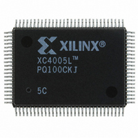
XC4005L-5PQ100C Xilinx Inc, XC4005L-5PQ100C Datasheet - Page 4

XC4005L-5PQ100C
Manufacturer Part Number
XC4005L-5PQ100C
Description
IC 3.3V FPGA 196 CLB'S 100-PQFP
Manufacturer
Xilinx Inc
Series
XC4000r
Datasheet
1.XC4005L-5PC84C.pdf
(175 pages)
Specifications of XC4005L-5PQ100C
Number Of Logic Elements/cells
466
Number Of Labs/clbs
196
Total Ram Bits
6272
Number Of I /o
77
Number Of Gates
5000
Voltage - Supply
3 V ~ 3.6 V
Mounting Type
Surface Mount
Operating Temperature
0°C ~ 85°C
Package / Case
100-BQFP
Lead Free Status / RoHS Status
Contains lead / RoHS non-compliant
Other names
122-1121
Available stocks
Company
Part Number
Manufacturer
Quantity
Price
XC4000 Series Field Programmable Gate Arrays
XC4000E and XC4000EX Families
Compared to the XC4000
For readers already familiar with the XC4000 family of Xil-
inx Field Programmable Gate Arrays, the major new fea-
tures in the XC4000-Series devices are listed in this
section.
XC4000EX devices are significantly increased system
speed, greater capacity, and new architectural features,
particularly Select-RAM memory. The XC4000EX devices
also offer many new routing features, including special
high-speed clock buffers that can be used to capture input
data with minimal delay.
Any XC4000E device is pinout- and bitstream-compatible
with the corresponding XC4000 device.
XC4000 bitstream can be used to program an XC4000E
device. However, since the XC4000E includes many new
features, an XC4000E bitstream cannot be loaded into an
XC4000 device.
Most XC4000EX devices have no corresponding XC4000
devices, because of the larger CLB arrays. The XC4028EX
has the same array size as the XC4025 and XC4025E, but
is not bitstream-compatible.
XC4025E, and XC4028EX are all pinout-compatible.
Improvements in XC4000E and XC4000EX
Increased System Speed
Delays in FPGA-based designs are layout dependent.
There is a rule of thumb designers can consider—the sys-
tem clock rate should not exceed one third to one half of the
specified toggle rate. Critical portions of a design, such as
shift registers and simple counters, can run faster—approx-
imately two thirds of the specified toggle rate.
XC4000E and XC4000EX devices can run at synchronous
system clock rates of up to 66 MHz, and internal perfor-
mance can exceed 150 MHz. This increase in performance
over the previous families stems from improvements in both
device processing and system architecture.
Series devices use a sub-micron triple-layer metal process.
In addition, many architectural improvements have been
made, as described below.
PCI Compliance
XC4000-Series -3 and faster speed grades are fully PCI
compliant. XC4000E and XC4000EX devices can be used
to implement a one-chip PCI solution.
Carry Logic
The speed of the carry logic chain has increased dramati-
cally. Some parameters, such as the delay on the carry
chain through a single CLB (T
much as 50% from XC4000 values. See
on page 21
4-8
The biggest advantages of XC4000E and
for more information.
BYP
However, the XC4025,
), have improved by as
“Fast Carry Logic”
An existing
XC4000-
Select-RAM Memory: Edge-Triggered, Synchronous
RAM Modes
The RAM in any CLB can be configured for synchronous,
edge-triggered, write operation. The read operation is not
affected by this change to an edge-triggered write.
Dual-Port RAM
A separate option converts the 16x2 RAM in any CLB into a
16x1 dual-port RAM with simultaneous Read/Write.
The function generators in each CLB can be configured as
either level-sensitive (asynchronous) single-port RAM,
edge-triggered (synchronous) single-port RAM, edge-trig-
gered (synchronous) dual-port RAM, or as combinatorial
logic.
Configurable RAM Content
The RAM content can now be loaded at configuration time,
so that the RAM starts up with user-defined data.
H Function Generator
In XC4000-Series devices, the H function generator is
more versatile than in the XC4000. Its inputs can come not
only from the F and G function generators but also from up
to three of the four control input lines. The H function gen-
erator can thus be totally or partially independent of the
other two function generators, increasing the maximum
capacity of the device.
IOB Clock Enable
The two flip-flops in each IOB have a common clock enable
input, which through configuration can be activated individ-
ually for the input or output flip-flop or both. This clock
enable operates exactly like the EC pin on the XC4000
CLB. This new feature makes the IOBs more versatile, and
avoids the need for clock gating.
Output Drivers
The output pull-up structure defaults to a TTL-like totem-
pole. This driver is an n-channel pull-up transistor, pulling
to a voltage one transistor threshold below Vcc, just like the
XC4000 outputs. Alternatively, XC4000-Series devices can
be globally configured with CMOS outputs, with p-channel
pull-up transistors pulling to Vcc. Also, the configurable pull-
up resistor in the XC4000 Series is a p-channel transistor
that pulls to Vcc, whereas in the XC4000 it is an n-channel
transistor that pulls to a voltage one transistor threshold
below Vcc.
Input Thresholds
The input thresholds can be globally configured for either
TTL (1.2 V threshold) or CMOS (2.5 V threshold), just like
XC2000 and XC3000 inputs. The two global adjustments of
input threshold and output level are independent of each
other.
September 18, 1996 (Version 1.04)


