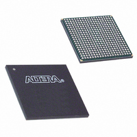
EP1C20F400C6N Altera, EP1C20F400C6N Datasheet - Page 91

EP1C20F400C6N
Manufacturer Part Number
EP1C20F400C6N
Description
IC CYCLONE FPGA 20K LE 400-FBGA
Manufacturer
Altera
Series
Cyclone®r
Datasheet
1.EP1C3T144C8.pdf
(106 pages)
Specifications of EP1C20F400C6N
Number Of Logic Elements/cells
20060
Number Of Labs/clbs
2006
Total Ram Bits
294912
Number Of I /o
301
Voltage - Supply
1.425 V ~ 1.575 V
Mounting Type
Surface Mount
Operating Temperature
0°C ~ 85°C
Package / Case
400-FBGA
Family Name
Cyclone®
Number Of Logic Blocks/elements
20060
# I/os (max)
301
Frequency (max)
405.2MHz
Process Technology
0.13um (CMOS)
Operating Supply Voltage (typ)
1.5V
Logic Cells
20060
Ram Bits
294912
Operating Supply Voltage (min)
1.425V
Operating Supply Voltage (max)
1.575V
Operating Temp Range
0C to 85C
Operating Temperature Classification
Commercial
Mounting
Surface Mount
Pin Count
400
Package Type
FBGA
Lead Free Status / RoHS Status
Lead free / RoHS Compliant
Number Of Gates
-
Lead Free Status / Rohs Status
Compliant
Other names
544-1687
Available stocks
Company
Part Number
Manufacturer
Quantity
Price
Company:
Part Number:
EP1C20F400C6N
Manufacturer:
ALTERA
Quantity:
237
Altera Corporation
May 2008
LVCMOS
3.3-V LVTTL
2.5-V LVTTL
1.8-V LVTTL
1.5-V LVTTL
SSTL-3 class I
SSTL-3 class II
SSTL-2 class I
Table 4–40. Cyclone I/O Standard Column Pin Input Delay Adders (Part 1 of 2)
I/O Standard
External I/O Delay Parameters
External I/O delay timing parameters for I/O standard input and output
adders and programmable input and output delays are specified by
speed grade independent of device density.
Tables 4–40
and row I/O pins for all packages. If an I/O standard is selected other
than LVTTL 4 mA with a fast slew rate, add the selected delay to the
external t
4–28.
t
t
t
t
t
t
t
t
t
t
I N S U
I N H
O U T C O
X Z
Z X
I N S U P L L
I N H P L L
O U T C O P L L
X Z P L L
Z X P L L
Table 4–39. EP1C20 Row Pin Global Clock External I/O Timing Parameters
-6 Speed Grade
Min
Symbol
—
—
—
—
—
—
—
—
CO
through
–250
–250
–278
and t
Max
182
278
27
-6 Speed Grade
2.417
0.000
2.000
1.417
0.000
0.500
0
0
Min
—
—
—
—
SU
I/O parameters shown in
4–45
3.724
3.645
3.645
1.667
1.588
1.588
Max
-7 Speed Grade
Min
—
—
—
—
—
—
—
—
—
—
—
—
show the adder delays associated with column
-7 Speed Grade
2.779
0.000
2.000
1.629
0.000
0.500
Min
—
—
—
—
–288
–288
–320
Max
209
319
31
0
0
4.282
4.191
4.191
1.917
1.826
1.826
Max
—
—
—
—
-8 Speed Grade
Min
Tables 4–25
—
—
—
—
—
—
—
—
-8 Speed Grade
3.140
0.000
2.000
1.840
0.000
0.500
Min
—
—
—
—
–325
–325
–362
Max
236
361
35
0
0
through
4.843
4.740
4.740
2.169
2.066
2.066
Max
Timing Model
—
—
—
—
Preliminary
Unit
ps
ps
ps
ps
ps
ps
ps
ps
Unit
ns
ns
ns
ns
ns
ns
ns
ns
ns
ns
4–21


